PIC16F/LF1946/47
28.1 Read-Modify-Write Operations
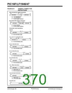
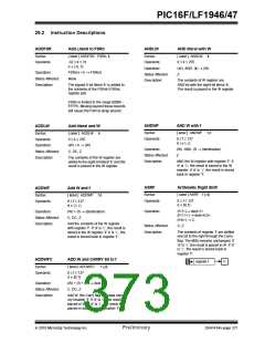
28.0 INSTRUCTION SET SUMMARY
Any instruction that specifies a file register as part of
the instruction performs a Read-Modify-Write (R-M-W)
operation. The register is read, the data is modified,
and the result is stored according to either the instruc-
tion, or the destination designator ‘d’. A read operation
is performed on a register even if the instruction writes
to that register.
Each PIC16 instruction is a 14-bit word containing the
operation code (opcode) and all required operands.
The opcodes are broken into three broad categories.
• Byte Oriented
• Bit Oriented
• Literal and Control
The literal and control category contains the most var-
ied instruction word format.
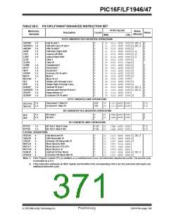
TABLE 28-1: OPCODE FIELD
DESCRIPTIONS
Table 28-3 lists the instructions recognized by the
MPASMTM assembler.
Field
Description
All instructions are executed within a single instruction
cycle, with the following exceptions, which may take
two or three cycles:
f
W
b
Register file address (0x00 to 0x7F)
Working register (accumulator)
Bit address within an 8-bit file register
Literal field, constant data or label
• Subroutine takes two cycles (CALL, CALLW)
• Returns from interrupts or subroutines take two
cycles (RETURN, RETLW, RETFIE)
k
x
Don’t care location (= 0or 1).
• Program branching takes two cycles (GOTO, BRA,
BRW, BTFSS, BTFSC, DECFSZ, INCSFZ)
• One additional instruction cycle will be used when
any instruction references an indirect file register
and the file select register is pointing to program
memory.
The assembler will generate code with x = 0.
It is the recommended form of use for
compatibility with all Microchip software tools.
d
Destination select; d = 0: store result in W,
d = 1: store result in file register f.
Default is d = 1.
One instruction cycle consists of 4 oscillator cycles; for
an oscillator frequency of 4 MHz, this gives a nominal
instruction execution rate of 1 MHz.
n
FSR or INDF number. (0-1)
mm
Pre-post increment-decrement mode
selection
All instruction examples use the format ‘0xhh’ to
represent a hexadecimal number, where ‘h’ signifies a
hexadecimal digit.
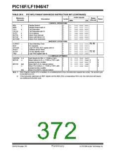
TABLE 28-2: ABBREVIATION
DESCRIPTIONS
Field
Description
PC
TO
C
Program Counter
Time-out bit
Carry bit
DC
Z
Digit carry bit
Zero bit
PD
Power-down bit
2010 Microchip Technology Inc.
Preliminary
DS41414A-page 367

 MICROCHIP [ MICROCHIP ]