PIC16F/LF1946/47
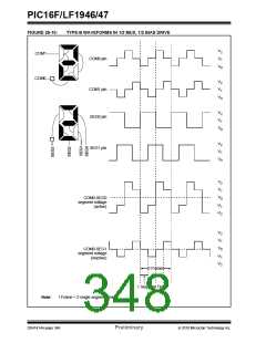
26.5 LCD Multiplex Types
26.7 Pixel Control
The LCD driver module can be configured into one of
four multiplex types:
The LCDDATAx registers contain bits which define the
state of each pixel. Each bit defines one unique pixel.
• Static (only COM0 is used)
Register 26-6 shows the correlation of each bit in the
LCDDATAx registers to the respective common and
segment signals.
• 1/2 multiplex (COM<1:0> are used)
• 1/3 multiplex (COM<2:0> are used)
• 1/4 multiplex (COM<3:0> are used)
Any LCD pixel location not being used for display can
be used as general purpose RAM.
The LMUX<1:0> bit setting of the LCDCON register
decides which of the LCD common pins are used (see
Table 26-4 for details).
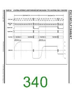
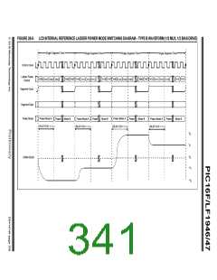
26.8 LCD Frame Frequency
The rate at which the COM and SEG outputs change is
called the LCD frame frequency.
If the pin is a digital I/O, the corresponding TRIS bit
controls the data direction. If the pin is a COM drive,
then the TRIS setting of that pin is overridden.
TABLE 26-5: FRAME FREQUENCY
FORMULAS
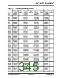
TABLE 26-4: COMMON PIN USAGE
LMUX
Multiplex
Frame Frequency =
Multiplex
COM3
COM2
COM1
<1:0>
Static
1/2
Clock source/(4 x 1 x (LPD Prescaler) x 32))
Clock source/(2 x 2 x (LPD Prescaler) x 32))
Clock source/(1 x 3 x (LPD Prescaler) x 32))
Clock source/(1 x 4 x (LPD Prescaler) x 32))
Static
1/2
00
01
10
11
Unused
Unused
Unused
Active
Unused
Unused
Active
Unused
Active
Active
Active
1/3
1/3
1/4
1/4
Active
Note:
Clock source is FOSC/256, T1OSC or
LFINTOSC.
26.6 Segment Enables
TABLE 26-6: APPROXIMATE FRAME
FREQUENCY (IN Hz) USING
FOSC @ 8 MHz, TIMER1 @
The LCDSEn registers are used to select the pin
function for each segment pin. The selection allows
each pin to operate as either an LCD segment driver or
as one of the pin’s alternate functions. To configure the
pin as a segment pin, the corresponding bits in the
LCDSEn registers must be set to ‘1’.
32.768 kHz OR LFINTOSC
LP<3:0>
Static
1/2
1/3
1/4
2
3
4
5
6
7
122
81
61
49
41
35
122
81
61
49
41
35
162
108
81
122
81
61
49
41
35
If the pin is a digital I/O, the corresponding TRIS bit
controls the data direction. Any bit set in the LCDSEn
registers overrides any bit settings in the corresponding
TRIS register.
65
Note:
On a Power-on Reset, these pins are
configured as normal I/O, not LCD pins.
54
47
DS41414A-page 342
Preliminary
2010 Microchip Technology Inc.

 MICROCHIP [ MICROCHIP ]