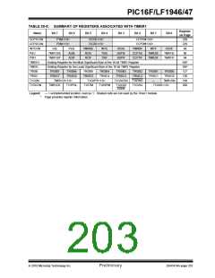
PIC16F/LF1946/47
20.11 Timer1 Control Register
The Timer1 Control register (T1CON), shown in
Register 20-1, is used to control Timer1 and select the
various features of the Timer1 module.
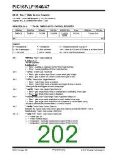
REGISTER 20-1: T1CON: TIMER1 CONTROL REGISTER
R/W-0/u
R/W-0/u
R/W-0/u
R/W-0/u
R/W-0/u
R/W-0/u
T1SYNC
U-0
—
R/W-0/u
TMR1CS<1:0>
T1CKPS<1:0>
T1OSCEN
TMR1ON
bit 7
bit 0
Legend:
R = Readable bit
W = Writable bit
U = Unimplemented bit, read as ‘0’
-n/n = Value at POR and BOR/Value at all other Resets
u = Bit is unchanged
‘1’ = Bit is set
x = Bit is unknown
‘0’ = Bit is cleared
bit 7-6
TMR1CS<1:0>: Timer1 Clock Source Select bits
11=Timer1 clock source is Capacitive Sensing Oscillator (CAPOSC)
10=Timer1 clock source is pin or oscillator:
If T1OSCEN = 0:
External clock from T1CKI pin (on the rising edge)
If T1OSCEN = 1:
Crystal oscillator on T1OSI/T1OSO pins
01=Timer1 clock source is system clock (FOSC)
00=Timer1 clock source is instruction clock (FOSC/4)
bit 5-4
T1CKPS<1:0>: Timer1 Input Clock Prescale Select bits
11= 1:8 Prescale value
10= 1:4 Prescale value
01= 1:2 Prescale value
00= 1:1 Prescale value
bit 3
bit 2
T1OSCEN: LP Oscillator Enable Control bit
1= Dedicated Timer1 oscillator circuit enabled
0= Dedicated Timer1 oscillator circuit disabled
T1SYNC: Timer1 External Clock Input Synchronization Control bit
TMR1CS<1:0> = 1X
1= Do not synchronize external clock input
0= Synchronize external clock input with system clock (FOSC)
TMR1CS<1:0> = 0X
This bit is ignored. Timer1 uses the internal clock when TMR1CS<1:0> = 1X.
bit 1
bit 0
Unimplemented: Read as ‘0’
TMR1ON: Timer1 On bit
1= Enables Timer1
0= Stops Timer1
Clears Timer1 Gate flip-flop
2010 Microchip Technology Inc.
Preliminary
DS41414A-page 199

 MICROCHIP [ MICROCHIP ]