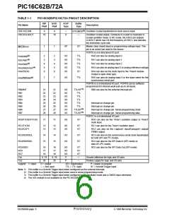
PIC16C62B/72A
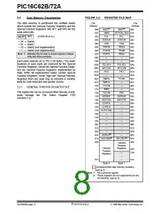
TABLE 2-1
Addr
SPECIAL FUNCTION REGISTER SUMMARY (Cont.’d)
Value on: Value on all
Name
Bit 7
Bit 6
Bit 5
Bit 4
Bit 3
Bit 2
Bit 1
Bit 0
POR,
BOR
other resets
(4)
Bank 1
80h
INDF(1)
Addressing this location uses contents of FSR to address data memory (not a physical register) 0000 0000 0000 0000
81h
OPTION_REG
PCL(1)
STATUS(1)
FSR(1)
TRISA
TRISB
TRISC
—
RBPU
Program Counter’s (PC) Least Significant Byte
IRP(5) RP1(5)
RP0 TO
Indirect data memory address pointer
PORTA Data Direction Register
INTEDG
T0CS
T0SE
PSA
PS2
PS1
PS0
1111 1111 1111 1111
0000 0000 0000 0000
0001 1xxx 000q quuu
xxxx xxxx uuuu uuuu
--11 1111 --11 1111
1111 1111 1111 1111
1111 1111 1111 1111
82h
83h
PD
Z
DC
C
84h
85h
—
—
86h
PORTB Data Direction Register
PORTC Data Direction Register
Unimplemented
87h
88h-89h
8Ah
—
—
PCLATH(1,2)
INTCON(1)
PIE1
—
GIE
—
—
—
T0IE
—
Write Buffer for the upper 5 bits of the Program Counter
---0 0000 ---0 0000
0000 000x 0000 000u
8Bh
PEIE
INTE
—
RBIE
T0IF
INTF
RBIF
8Ch
8Dh
8Eh
ADIE(3)
SSPIE
CCP1IE
TMR2IE
TMR1IE -0-- 0000 -0-- 0000
—
Unimplemented
—
—
—
PCON
—
—
—
—
—
POR
BOR
---- --qq ---- --uu
8Fh-91h
92h
—
Unimplemented
—
—
PR2
Timer2 Period Register
Synchronous Serial Port (I2C mode) Address Register
1111 1111 1111 1111
0000 0000 0000 0000
0000 0000 0000 0000
93h
SSPADD
SSPSTAT
—
94h
SMP
CKE
D/A
P
S
R/W
UA
BF
95h-9Eh
9Fh
Unimplemented
—
—
—
ADCON1(3)
—
—
—
—
PCFG2
PCFG1
PCFG0 ---- -000 ---- -000
Legend: x= unknown, u= unchanged, q= value depends on condition, -= unimplemented, read as ’0’,
Shaded locations are unimplemented, read as ’0’.
Note 1: These registers can be addressed from either bank.
2: The upper byte of the program counter is not directly accessible. PCLATH is a holding register for PC<12:8> whose contents
are transferred to the upper byte of the program counter.
3: A/D not implemented on the PIC16C62B, maintain as ’0’.
4: Other (non power-up) resets include: external reset through MCLR and the Watchdog Timer Reset.
5: The IRP and RP1 bits are reserved. Always maintain these bits clear.
6: On any device reset, these pins are configured as inputs.
7: This is the value that will be in the port output latch.
DS35008B-page 10
Preliminary
1999 Microchip Technology Inc.

 MICROCHIP [ MICROCHIP ]