PIC12F683
this data sheet and is highly recommended reading for
a better understanding of the device architecture and
operation of the peripheral modules.
1.0
DEVICE OVERVIEW
This document contains device specific information for
the PIC12F683. Additional information may be found in
the “PICmicro® Mid-Range MCU Family Reference
Manual” (DS33023), which may be obtained from your
local Microchip Sales Representative or downloaded
from the Microchip web site. The reference manual
should be considered a complementary document to
The PIC12F683 is covered by this data sheet. It is
available in 8-pin PDIP, SOIC and DFN-S packages.
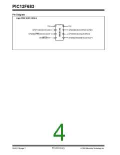
Figure 1-1 shows a block diagram of the PIC12F683
device. Table 1-1 shows the pinout description.
FIGURE 1-1:
PIC12F683 BLOCK DIAGRAM
INT
Configuration
13
8
Data Bus
Program Counter
GP0
GP1
Flash
2k x 14
Program
GP2
RAM
GP3
Memory
8-Level Stack
(13-bit)
128 bytes
GP4
File
Registers
GP5
Program
Bus
14
RAM Addr
9
Addr MUX
Instruction reg
Indirect
Addr
7
Direct Addr
8
FSR reg
Status reg
MUX
8
3
Power-up
Timer
Instruction
Decode &
Control
Oscillator
Start-up Timer
ALU
Power-on
Reset
8
Timing
Generation
Watchdog
Timer
OSC1/CLKIN
W reg
Brown-out
Detect
OSC2/CLKOUT
Internal
Oscillator
Block
CCP1
CCP
T1G
VDD
VSS
MCLR
T1CKI
Timer0
Timer1
Timer2
T0CKI
1 Analog Comparator
and Reference
Analog-to-Digital Converter
EEDATA
256 bytes
Data
8
EEPROM
EEADDR
VREF
CIN- CIN+ COUT
AN0 AN1 AN2 AN3
2004 Microchip Technology Inc.
Preliminary
DS41211B-page 5

 MICROCHIP [ MICROCHIP ]