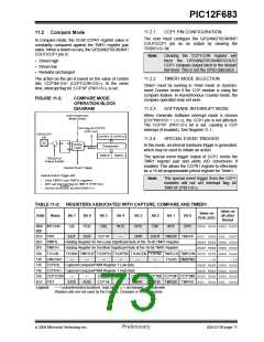
PIC12F683
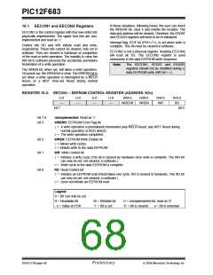
After a write sequence has been initiated, clearing the
WREN bit will not affect this write cycle. The WR bit will
be inhibited from being set unless the WREN bit is set.
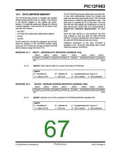
10.2 Reading the EEPROM Data
Memory
To read a data memory location, the user must write the
address to the EEADR register and then set control bit
RD (EECON1<0>), as shown in Example 10-1. The
data is available, in the very next cycle, in the EEDAT
register. Therefore, it can be read in the next
instruction. EEDAT holds this value until another read,
or until it is written to by the user (during a write
operation).
At the completion of the write cycle, the WR bit is
cleared in hardware and the EE Write Complete
Interrupt Flag bit (EEIF) is set. The user can either
enable this interrupt or poll this bit. The EEIF bit
(PIR1<7>) must be cleared by software.
10.4 Write Verify
Depending on the application, good programming
practice may dictate that the value written to the data
EEPROM should be verified (see Example 10-3) to the
desired value to be written.
EXAMPLE 10-1:
DATA EEPROM READ
BSF
STATUS,RP0
CONFIG_ADDR
EEADR
EECON1,RD
EEDAT,W
;Bank 1
;
;Address to read
;EE Read
;Move data to W
MOVLW
MOVWF
BSF
EXAMPLE 10-3:
WRITE VERIFY
MOVF
BSF
STATUS,RP0 ;Bank 1
MOVF
EEDAT,W
;EEDAT not changed
;from previous write
;YES, Read the
;value written
10.3 Writing to the EEPROM Data
Memory
BSF
EECON1,RD
XORWF
BTFSS
GOTO
:
EEDAT,W
STATUS,Z
WRITE_ERR
To write an EEPROM data location, the user must first
write the address to the EEADR register and the data
to the EEDAT register. Then the user must follow a
specific sequence to initiate the write for each byte, as
shown in Example 10-2.
;Is data the same
;No, handle error
;Yes, continue
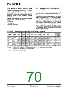
10.4.1
USING THE DATA EEPROM
EXAMPLE 10-2:
DATA EEPROM WRITE
The data EEPROM is a high-endurance, byte address-
able array that has been optimized for the storage of
frequently changing information. The maximum endur-
ance for any EEPROM cell is specified as Dxxx. D120
or D120A specify a maximum number of writes to any
EEPROM location before a refresh is required of
infrequently changing memory locations.
BSF
STATUS,RP0
;Bank 1
BSF
EECON1,WREN ;Enable write
BCF
INTCON,GIE
55h
EECON2
AAh
EECON2
;Disable INTs
;Unlock write
;
;
MOVLW
MOVWF
MOVLW
MOVWF
BSF
;
EECON1,WR
INTCON,GIE
;Start the write
;Enable INTS
10.4.1.1
EEPROM Endurance
BSF
A hypothetical data EEPROM is 64 bytes long and has
an endurance of 1M writes. It also has a refresh param-
eter of 10M writes. If every memory location in the cell
were written the maximum number of times, the data
EEPROM would fail after 64M write cycles. If every
memory location, save one, were written the maximum
number of times, the data EEPROM would fail after
63M write cycles but the one remaining location could
fail after 10M cycles. If proper refreshes occurred, then
the lone memory location would have to be refreshed
six times for the data to remain correct.
The write will not initiate if the above sequence is not
exactly followed (write 55h to EECON2, write AAh to
EECON2, then set WR bit) for each byte. We strongly
recommend that interrupts be disabled during this
code segment. A cycle count is executed during the
required sequence. Any number that is not equal to the
required cycles to execute the required sequence will
prevent the data from being written into the EEPROM.
Additionally, the WREN bit in EECON1 must be set to
enable write. This mechanism prevents accidental
writes to data EEPROM due to errant (unexpected)
code execution (i.e., lost programs). The user should
keep the WREN bit clear at all times, except when
updating EEPROM. The WREN bit is not cleared
by hardware.
2004 Microchip Technology Inc.
Preliminary
DS41211B-page 67

 MICROCHIP [ MICROCHIP ]