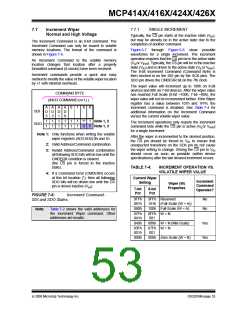
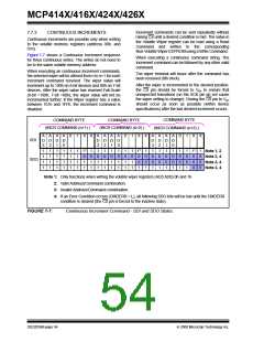
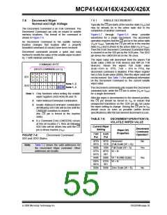
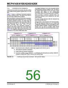
MCP414X/416X/424X/426X
7.9.1
SINGLE ENABLE WRITE PROTECT
OR WIPERLOCK TECHNOLOGY
(HIGH VOLTAGE)
7.9
Modify Write Protect or WiperLock
Technology (High Voltage)
Enable and Disable
Figure 6-7 through Figure 6-8 show possible
waveforms for a single Modify Write Protect or
WiperLock Technology command.
This command is a special case of the High Voltage
Decrement Wiper and High Voltage Increment Wiper
commands to the non-volatile memory locations 02h,
03h, and 0Fh. This command is used to enable or
disable either the software Write Protect, wiper 0
WiperLock Technology, or wiper 1 WiperLock Technol-
ogy. Table 7-6 shows the memory addresses, the High
Voltage command and the result of those commands
on the non-volatile WP, WL0, 0r WL1 bits. The format
of the command is shown in Figure 7-8 (Enable) or
Figure 7-6 (Disable).
A Modify Write Protect or WiperLock Technology
Command will only start an EEPROM write cycle (twc
)
after a properly formatted Command (8-clocks) has
been received and the CS pin transitions to the inactive
state (VIH).
After the CS pin is driven inactive (VIH), the serial
interface may immediately be re-enabled by driving the
CS pin to the active state (VILor VIHH).
During an EEPROM write cycle, only serial commands
to Volatile memory (addresses 00h, 01h, 04h, and 05h)
are accepted. All other serial commands are ignored
until the EEPROM write cycle (twc) completes. This
allows the Host Controller to operate on the Volatile
Wiper registers and the TCON register, and to Read
the Status Register. The EEWA bit in the Status register
indicates the status of an EEPROM Write Cycle.
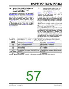
TABLE 7-6:
ADDRESS MAP TO MODIFY WRITE PROTECT AND WIPERLOCK TECHNOLOGY
Command’s and Result
Memory
Address
High Voltage Decrement Wiper
High Voltage Increment Wiper
00h
01h
Wiper 0 register is decremented
Wiper 1 register is decremented
WL0 is enabled
Wiper 0 register is incremented
Wiper 1 register is incremented
WL0 is disabled
02h
03h
WL1 is enabled
WL1 is disabled
04h (1)
05h - 0Eh (1)
0Fh
TCON register not changed, CMDERR bit is set TCON register not changed, CMDERR bit is set
Reserved
Reserved
WP is enabled
WP is disabled
Note 1: Reserved addresses: Increment or Decrement commands are invalid for these addresses.
© 2008 Microchip Technology Inc.
DS22059B-page 57

 MICROCHIP [ MICROCHIP ]