MCP414X/416X/424X/426X
8.2
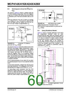
Techniques to force the CS pin to
VIHH
PIC10F206
R1
GP0
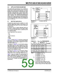
The circuit in Figure 8-3 shows a method using the
TC1240A doubling charge pump. When the SHDN pin
is high, the TC1240A is off, and the level on the CS pin
is controlled by the PIC® microcontrollers (MCUs) IO2
pin.
MCP4XXX
GP2
CS
C1
When the SHDN pin is low, the TC1240A is on and the
VOUT voltage is 2 * VDD. The resistor R1 allows the CS
pin to go higher than the voltage such that the PIC
C2
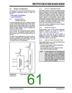
FIGURE 8-4:
MCP4XXX Non-volatile
MCU’s IO2 pin “clamps” at approximately VDD
.
Digital Potentiometer Evaluation Board
(MCP402XEV) implementation to generate the
TC1240A
VIN
V
voltage.
IHH
C+
PIC MCU
C1
C-
SHDN
8.3
Using Shutdown Modes
VOUT
IO1
Figure 8-5 shows a possible application circuit where
the independent terminals could be used.
Disconnecting the wiper allows the transistor input to
be taken to the Bias voltage level (disconnecting A and
or B may be desired to reduce system current).
Disconnecting Terminal A modifies the transistor input
by the RBW rheostat value to the Common B.
Disconnecting Terminal B modifies the transistor input
by the RAW rheostat value to the Common A. The
Common A and Common B connections could be
MCP402X
R1
CS
IO2
C2
FIGURE 8-3:
generate the V
Using the TC1240A to
voltage.
IHH
connected to VDD and VSS
.
The circuit in Figure 8-4 shows the method used on the
MCP402X Non-volatile Digital Potentiometer Evalua-
tion Board (Part Number: MCP402XEV). This method
requires that the system voltage be approximately 5V.
This ensures that when the PIC10F206 enters a
brown-out condition, there is an insufficient voltage
level on the CS pin to change the stored value of the
wiper. The MCP402X Non-volatile Digital Potentiome-
ter Evaluation Board User’s Guide (DS51546) contains
a complete schematic.
Common A
Input
A
GP0 is a general purpose I/O pin, while GP2 can either
be a general purpose I/O pin or it can output the internal
clock.
To base
of Transistor
(or Amplifier)
W
For the serial commands, configure the GP2 pin as an
input (high impedance). The output state of the GP0 pin
will determine the voltage on the CS pin (VIL or VIH).
For high-voltage serial commands, force the GP0
output pin to output a high level (VOH) and configure the
GP2 pin to output the internal clock. This will form a
charge pump and increase the voltage on the CS pin
(when the system voltage is approximately 5V).
B
Input
Common B
Balance
Bias
Example Application Circuit
FIGURE 8-5:
using Terminal Disconnects.
DS22059B-page 60
© 2008 Microchip Technology Inc.

 MICROCHIP [ MICROCHIP ]