MCP414X/416X/424X/426X
7.1
Command Byte
7.0
DEVICE COMMANDS
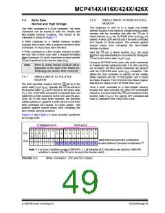
The Command Byte has three fields, the Address, the
Command, and 2 Data bits, see Figure 7-1. Currently
only one of the data bits is defined (D8). This is for the
Write command.
The MCP4XXX’s SPI command format supports 16
memory address locations and four commands. Each
command has two modes. These are:
• Normal Serial Commands
The device memory is accessed when the master
sends a proper Command Byte to select the desired
operation. The memory location getting accessed is
contained in the Command Byte’s AD3:AD0 bits. The
action desired is contained in the Command Byte’s
C1:C0 bits, see Table 7-1. C1:C0 determines if the
desired memory location will be read, written,
Incremented (wiper setting +1) or Decremented (wiper
setting -1). The Increment and Decrement commands
are only valid on the volatile wiper registers, and in
High Voltage commands to enable/disable WiperLock
Technology and Software Write Protect.
• High-Voltage Serial Commands
Normal serial commands are those where the CS pin is
driven to VIL. With High-Voltage Serial Commands, the
CS pin is driven to VIHH. In each mode, there are four
possible commands. These commands are shown in
Table 7-1.
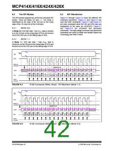
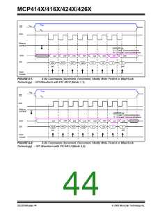
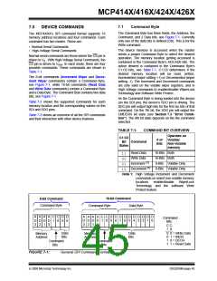
The 8-bit commands (Increment Wiper and Decre-
ment Wiper commands) contain a Command Byte,
see Figure 7-1, while 16-bit commands (Read Data
and Write Data commands) contain a Command Byte
and a Data Byte. The Command Byte contains two data
bits, see Figure 7-1.
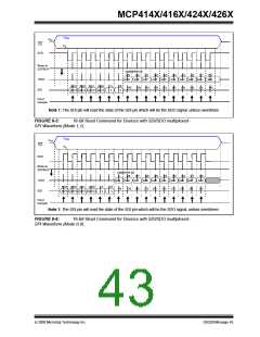
As the Command Byte is being loaded into the device
(on the SDI pin), the device’s SDO pin is driving. The
SDO pin will output high bits for the first six bits of that
command. On the 7th bit, the SDO pin will output the
CMDERR bit state (see Section 7.3 “Error Condi-
tion”). The 8th bit state depends on the the command
selected.
Table 7-2 shows the supported commands for each
memory location and the corresponding values on the
SDI and SDO pins.
Table 7-3 shows an overview of all the SPI commands
and their interaction with other device features.
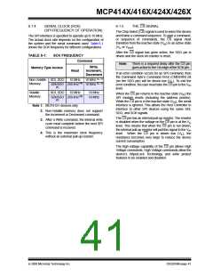
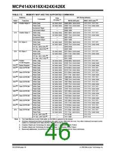
TABLE 7-1:
C1:C0
COMMAND BIT OVERVIEW
Operates on
# of
Bits
Volatile/
Non-Volatile
memory
Bit
Command
States
Read Data
16-Bits Both
11
00
01
10
Write Data
16-Bits Both
Increment (1)
Decrement (1)
8-Bits Volatile Only
8-Bits Volatile Only
Note 1: High Voltage Increment and Decrement
commands on select non-volatile memory
locations
enable/disable
WiperLock
Technology and the software Write
Protect feature.
16-bit Command
Data Byte
8-bit Command
Command Byte
Command Byte
A A A A C C D D D D D D D D D D
D D D D 1 0 9 8 7 6 5 4 3 2 1 0
3 2 1 0
A A A A C C D D
D D D D 1 0 9 8
3 2 1 0
Command
Bits
C C
1 0
Data
Bits
0 0 = Write Data
0 1 = INCR
Data
Bits
Memory
Address
Memory
Address
1 0 = DECR
1 1 = Read Data
Command
Bits
Command
Bits
FIGURE 7-1:
General SPI Command Formats.
© 2008 Microchip Technology Inc.
DS22059B-page 45

 MICROCHIP [ MICROCHIP ]