MCP414X/416X/424X/426X
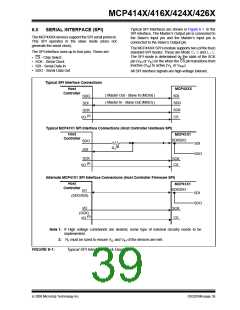
6.2
The SPI Modes
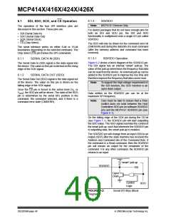
6.3
SPI Waveforms
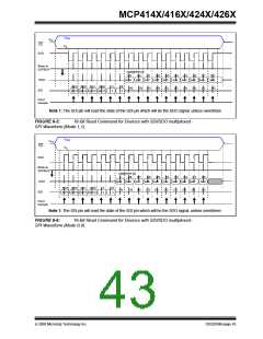
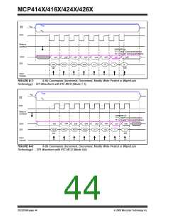
The SPI module supports two (of the four) standard SPI
modes. These are Mode 0,0 and 1,1. The mode is
determined by the state of the SDI pin on the rising
edge of the 1st clock bit (of the 8-bit byte).
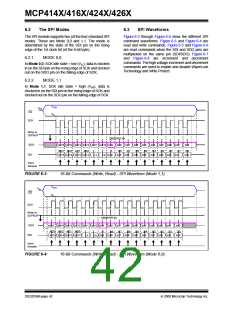
Figure 6-3 through Figure 6-8 show the different SPI
command waveforms. Figure 6-3 and Figure 6-4 are
read and write commands. Figure 6-5 and Figure 6-6
are read commands when the SDI and SDO pins are
multiplexed on the same pin (SDI/SDO). Figure 6-7
and Figure 6-8 are increment and decrement
commands. The high voltage increment and decrement
commands are used to enable and disable WiperLock
Technology and Write Protect.
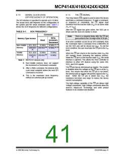
6.2.1
MODE 0,0
In Mode 0,0: SCK idle state = low (VIL), data is clocked
in on the SDI pin on the rising edge of SCK and clocked
out on the SDO pin on the falling edge of SCK.
6.2.2
MODE 1,1
In Mode 1,1: SCK idle state = high (VIH), data is
clocked in on the SDI pin on the rising edge of SCK and
clocked out on the SDO pin on the falling edge of SCK.
V
IHH
V
IH
CS
V
IL
SCK
Write to
SSPBUF
CMDERR bit
bit15 bit14 bit13 bit12 bit11 bit10 bit9 bit8 bit7 bit6 bit5
SDO
bit4 bit3 bit2 bit1
bit0
AD3 AD2 AD1 AD0
bit15 bit14 bit13 bit12
X
D8
D7
D6
D5
D4
D3
D2
D1
D0
SDI
bit9
bit8 bit7 bit6 bit5
bit4 bit3 bit2 bit1
bit0
C1
C0
Input
Sample
FIGURE 6-3:
16-Bit Commands (Write, Read) - SPI Waveform (Mode 1,1).
V
IHH
V
IH
CS
V
IL
SCK
Write to
SSPBUF
CMDERR bit
SDO
bit15 bit14 bit13 bit12 bit11 bit10 bit9
bit8 bit7 bit6 bit5
bit4 bit3 bit2 bit1
bit0
AD3 AD2 AD1 AD0
bit15 bit14 bit13 bit12
X
D8
D7
D6
D5
D4
D3
D2
D1
D0
SDI
bit9
bit8 bit7 bit6 bit5
bit4 bit3 bit2 bit1
bit0
C1
C0
Input
Sample
FIGURE 6-4:
16-Bit Commands (Write, Read) - SPI Waveform (Mode 0,0).
DS22059B-page 42
© 2008 Microchip Technology Inc.

 MICROCHIP [ MICROCHIP ]