MCP414X/416X/424X/426X
6.1.4
SERIAL CLOCK (SCK)
6.1.5
THE CS SIGNAL
(SPI FREQUENCY OF OPERATION)
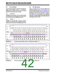
The Chip Select (CS) signal is used to select the device
and frame a command sequence. To start a command,
or sequence of commands, the CS signal must
transition from the inactive state (VIH) to an active state
(VIL or VIHH).
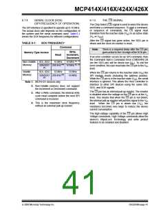
The SPI interface is specified to operate up to 10 MHz.
The actual clock rate depends on the configuration of
the system and the serial command used. Table 6-1
shows the SCK frequency for different configurations.
After the CS signal has gone active, the SDO pin is
driven and the clock bit counter is reset.
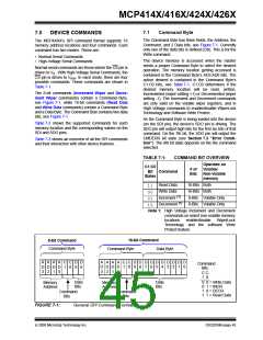
TABLE 6-1:
SCK FREQUENCY
Command
Write,
Note:
There is a required delay after the CS pin
goes active to the 1st edge of the SCK pin.
Memory Type Access
Read
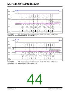
Increment,
Decrement
If an error condition occurs for an SPI command, then
the Command byte’s Command Error (CMDERR) bit
(on the SDO pin) will be driven low (VIL). To exit the
error condition, the user must take the CS pin to the VIH
level.
Non-Volatile SDI, SDO
Memory
10 MHz
10 MHz (2, 3)
SDI/SDO 250 kHz (4) 10 MHz (2, 3)
(1)
Volatile
Memory
SDI, SDO
10 MHz
10 MHz
10 MHz
When the CS pin returns to the inactive state (VIH) the
SPI module resets (including the address pointer).
While the CS pin is in the inactive state (VIH), the serial
interface is ignored. This allows the Host Controller to
interface to other SPI devices using the same SDI,
SDO, and SCK signals.
SDI/SDO 250 kHz (4)
(1)
Note 1: MCP41X1 devices only
2: Non-Volatile memory does not support
the Increment or Decrement command.
The CS pin has an internal pull-up resistor. The resistor
is disabled when the voltage on the CS pin is at the VIL
level. This means that when the CS pin is not driven,
the internal pull-up resistor will pull this signal to the VIH
level. When the CS pin is driven low (VIL), the
resistance becomes very large to reduce the device
current consumption.
3: After a Write command, the internal write
cycle must complete before the next SPI
command is received.
4: This is the maximum clock frequency
without an external pull-up resistor.
The high voltage capability of the CS pin allows High
Voltage commands. High Voltage commands allow the
device’s WiperLock Technology and write protect
features to be enabled and disabled.
© 2008 Microchip Technology Inc.
DS22059B-page 41

 MICROCHIP [ MICROCHIP ]