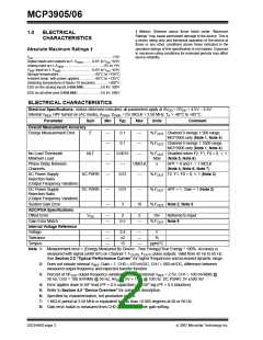
MCP3905/06
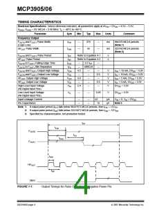
TIMING CHARACTERISTICS
Electrical Specifications: Unless otherwise indicated, all parameters apply at AVDD = DVDD = 4.5V – 5.5V,
AGND, DGND = 0V, MCLK = 3.58 MHz; TA = -40°C to +85°C.
Parameter
Frequency Output
OUT0 and FOUT1 Pulse Width
Sym
Min
Typ
Max
Units
Comment
F
tFW
tHW
—
275
90
—
—
ms
ms
984376 MCLK periods
(Note 1)
(Logic-Low)
HFOUT Pulse Width
—
322160 MCLK periods
(Note 2)
FOUT0 and FOUT1 Pulse Period
HFOUT Pulse Period
tFP
tHP
tFS2
tFS
Refer to Equation 4-1
Refer to Equation 4-2
s
s
FOUT0 to FOUT1 Falling-Edge Time
FOUT0 to FOUT1 Min Separation
FOUT0 and FOUT1 Output High Voltage
—
—
0.5 tFP
—
—
4/MCLK
VOH
VOL
VOH
VOL
VIH
4.5
—
—
—
—
—
—
—
V
V
V
V
V
IOH = 10 mA, DVDD = 5.0V
IOL = 10 mA, DVDD = 5.0V
IOH = 5 mA, DVDD = 5.0V
IOL = 5 mA, DVDD = 5.0V
DVDD = 5.0V
F
OUT0 and FOUT1 Output Low Voltage
0.5
—
HFOUT Output High Voltage
HFOUT Output Low Voltage
4.0
—
0.5
—
High-Level Input Voltage
(All Digital Input Pins)
2.4
Low-Level Input Voltage
(All Digital Input Pins)
VIL
—
—
0.85
V
DVDD = 5.0V
Input Leakage Current
Pin Capacitance
—
—
—
—
±3
10
µA
pF
VIN = 0, VIN = DVDD
Note 3
Note 1: If output pulse period (tFP) falls below 984376*2 MCLK periods, then tFW = 1/2 tFP
.
2: If output pulse period (tHP) falls below 322160*2 MCLK periods, then tHW = 1/2 tHP
.
3: Specified by characterization, not production tested.
tFP
tFW
FOUT0
tFS
tFS2
FOUT1
tHW
HFOUT
tHP
NEG
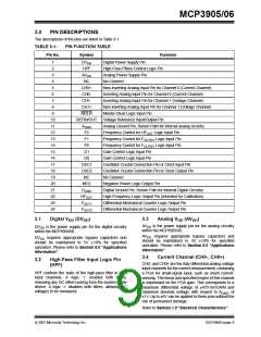
FIGURE 1-1:
Output Timings for Pulse Outputs and Negative Power Pin.
DS21948D-page 4
© 2007 Microchip Technology Inc.

 MICROCHIP [ MICROCHIP ]