MCP3905/06
ELECTRICAL CHARACTERISTICS (CONTINUED)
Electrical Specifications: Unless otherwise indicated, all parameters apply at AVDD = DVDD = 4.5V – 5.5V,
Internal VREF, HPF turned on (AC mode), AGND, DGND = 0V, MCLK = 3.58 MHz; TA = -40°C to +85°C.
Parameter
Reference Input
Sym
Min
Typ.
Max
Units
Comment
Input Range
2.2
3.2
—
—
—
—
2.6
—
V
Input Impedance
Input Capacitance
Analog Inputs
kΩ
pF
10
Maximum Signal Level
—
—
—
—
±1
V
CH0+,CH0-,CH1+,CH1- to AGND
G = PGA Gain on Channel 0
Differential Input Voltage
Range Channel 0
±470/G
mV
Differential Input Voltage
Range Channel 1
—
—
±660
mV
Input Impedance
390
—
—
—
—
kΩ
kHz
Proportional to 1/MCLK frequency
Bandwidth
(Notch Frequency)
14
Proportional to MCLK frequency,
MCLK/256
Oscillator Input
Frequency Range
Power Specifications
Operating Voltage
IDD,A
MCLK
1
—
4
MHz
4.5
—
—
5.5
3.0
2.0
V
AVDD, DVDD
AVDD pin only
DVDD pin only
IDD,A
IDD,D
2.7
1.2
mA
mA
IDD,D
—
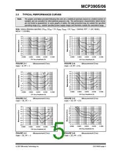
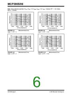
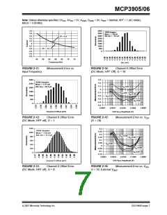
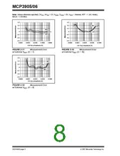
Note 1: Measurement error = (Energy Measured By Device - True Energy)/True Energy * 100%. Accuracy is
measured with signal (±660 mV) on Channel 1. FOUT0, FOUT1 pulse outputs. Valid from 45 Hz to 65 Hz.
See Section 2.0 “Typical Performance Curves” for higher frequencies and increased dynamic range.
2: Does not include internal VREF. Gain = 1, CH0 = 470 mVDC, CH1 = 660 mVDC, difference between
measured output frequency and expected transfer function.
3: Percent of HFOUT output frequency variation; Includes external VREF = 2.5V, CH1 = 100 mVRMS @
50 Hz, CH2 = 100 mVRMS @ 50 Hz, AVDD = 5V + 1Vpp @ 100 Hz. DC PSRR: 5V ±500 mV.
4: Error applies down to 60° lead (PF = 0.5 capacitive) and 60° lag (PF = 0.5 inductive).
5: Refer to Section 4.0 “Device Overview” for complete description.
6: Specified by characterization, not production tested.
7: 1 MCLK period at 3.58 MHz is equivalent to less than <0.005 degrees at 50 or 60 Hz.
8: Gain error match is measured from CH0 G = 1 to any other gain setting.
TEMPERATURE CHARACTERISTICS
Electrical Specifications: Unless otherwise indicated, VDD = 4.5V – 5.5V, AGND, DGND = 0V.
Parameters
Sym
Min
Typ
Max
Units
Conditions
Temperature Ranges
Specified Temperature Range
Operating Temperature Range
Storage Temperature Range
TA
TA
TA
-40
-40
-65
—
—
—
+85
+125
+150
°C
°C
°C
Note
Note:
The MCP3905/06 operate over this extended temperature range, but with reduced performance. In any
case, the Junction Temperature (TJ) must not exceed the Absolute Maximum specification of +150°C.
© 2007 Microchip Technology Inc.
DS21948D-page 3

 MICROCHIP [ MICROCHIP ]