MCP3905/06
† Notice: Stresses above those listed under "Maximum
Ratings" may cause permanent damage to the device. This is
a stress rating only and functional operation of the device at
those or any other conditions above those indicated in the
operation listings of this specification is not implied. Exposure
to maximum rating conditions for extended periods may affect
device reliability.
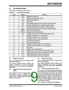
1.0
ELECTRICAL
CHARACTERISTICS
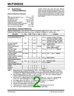
Absolute Maximum Ratings †
VDD ...................................................................................7.0V
Digital inputs and outputs w.r.t. A
........ -0.6V to VDD +0.6V
GND
Analog input w.r.t. A
.........................................-6V to +6V
GND
V
input w.r.t. A
............................... -0.6V to VDD +0.6V
REF
GND
Storage temperature .....................................-65°C to +150°C
Ambient temp. with power applied ................-65°C to +125°C
Soldering temperature of leads (10 seconds) .............+300°C
ESD on the analog inputs (HBM,MM).................5.0 kV, 500V
ESD on all other pins (HBM,MM)........................5.0 kV, 500V
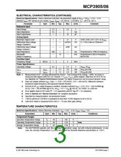
ELECTRICAL CHARACTERISTICS
Electrical Specifications: Unless otherwise indicated, all parameters apply at AVDD = DVDD = 4.5V – 5.5V,
Internal VREF, HPF turned on (AC mode), AGND, DGND = 0V, MCLK = 3.58 MHz; TA = -40°C to +85°C.
Parameter
Sym
Min
Typ.
Max
Units
Comment
Overall Measurement Accuracy
Energy Measurement Error
E
—
—
—
—
—
0.1
0.1
—
—
% FOUT Channel 0 swings 1:500 range,
MCP3905 only (Note 1, Note 4)
% FOUT Channel 0 swings 1:1000 range,
MCP3906 only (Note 1, Note 4)
No-Load Threshold/
Minimum Load
NLT
0.0015
—
—
% FOUT Disabled when F2, F1, F0 = 0, 1, 1
Max
(Note 5, Note 6)
Phase Delay Between
Channels
1/MCLK
—
s
HPF = 0 and 1, < 1 MCLK
(Note 4, Note 6, Note 7)
AC Power Supply
Rejection Ratio
(Output Frequency Variation)
AC PSRR
DC PSRR
0.01
% FOUT F2, F1, F0 = 0, 1, 1 (Note 3)
% FOUT HPF = 1, Gain = 1 (Note 3)
% FOUT Note 2, Note 5
DC Power Supply
Rejection Ratio
(Output Frequency Variation)
—
—
0.01
3
—
System Gain Error
ADC/PGA Specifications
Offset Error
10
VOS
—
—
2
5
mV
Referred to Input
Gain Error Match
Internal Voltage Reference
Voltage
0.5
—
% FOUT Note 8
—
—
—
2.4
±2
15
—
—
—
V
%
Tolerance
Tempco
ppm/°C
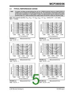
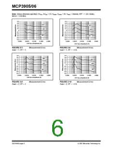
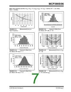
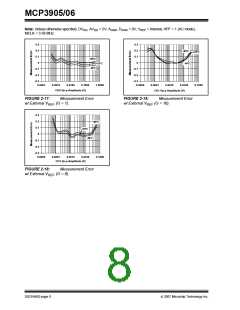
Note 1: Measurement error = (Energy Measured By Device - True Energy)/True Energy * 100%. Accuracy is
measured with signal (±660 mV) on Channel 1. FOUT0, FOUT1 pulse outputs. Valid from 45 Hz to 65 Hz.
See Section 2.0 “Typical Performance Curves” for higher frequencies and increased dynamic range.
2: Does not include internal VREF. Gain = 1, CH0 = 470 mVDC, CH1 = 660 mVDC, difference between
measured output frequency and expected transfer function.
3: Percent of HFOUT output frequency variation; Includes external VREF = 2.5V, CH1 = 100 mVRMS @
50 Hz, CH2 = 100 mVRMS @ 50 Hz, AVDD = 5V + 1Vpp @ 100 Hz. DC PSRR: 5V ±500 mV.
4: Error applies down to 60° lead (PF = 0.5 capacitive) and 60° lag (PF = 0.5 inductive).
5: Refer to Section 4.0 “Device Overview” for complete description.
6: Specified by characterization, not production tested.
7: 1 MCLK period at 3.58 MHz is equivalent to less than <0.005 degrees at 50 or 60 Hz.
8: Gain error match is measured from CH0 G = 1 to any other gain setting.
DS21948D-page 2
© 2007 Microchip Technology Inc.

 MICROCHIP [ MICROCHIP ]