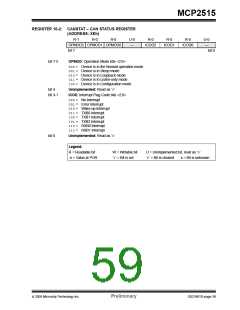
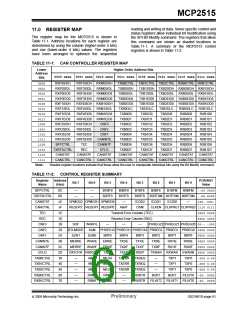
MCP2515
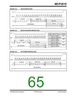
the Read instruction (i.e., sequential reads are
possible). This instruction further reduces the SPI
overhead by automatically clearing the associated
receive flag (CANINTF.RXnIF) when CS is raised at
the end of the command.
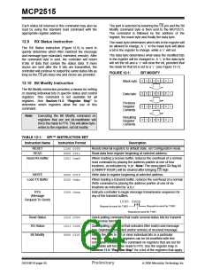
12.0 SPI™ INTERFACE
12.1 Overview
The MCP2515 is designed to interface directly with the
Serial Peripheral Interface (SPI) port available on many
microcontrollers and supports Mode 0,0 and Mode 1,1.
Commands and data are sent to the device via the SI
pin, with data being clocked in on the rising edge of
SCK. Data is driven out by the MCP2515 (on the SO
line) on the falling edge of SCK. The CS pin must be
held low while any operation is performed. Table 12-1
shows the instruction bytes for all operations. Refer to
Figure 12-10 and Figure 12-11 for detailed input and
output timing diagrams for both Mode 0,0 and Mode 1,1
operation.
12.5 Write Instruction
The Write instruction is started by lowering the CS pin.
The Write instruction is then sent to the MCP2515
followed by the address and at least one byte of data.
It is possible to write to sequential registers by
continuing to clock in data bytes, as long as CS is held
low. Data will actually be written to the register on the
rising edge of the SCK line for the D0 bit. If the CS line
is brought high before eight bits are loaded, the write
will be aborted for that data byte and previous bytes in
the command will have been written. Refer to the timing
diagram in Figure 12-4 for a more detailed illustration of
the byte write sequence.
Note:
The MCP2515 expects the first byte after
lowering CS to be the
instruction/command byte. This implies
that CS must be raised and then lowered
again to invoke another command.
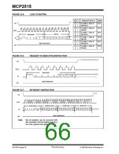
12.6 Load TX Buffer Instruction
12.2 Reset Instruction
The Load TX Buffer instruction (Figure 12-5) eliminates
the eight-bit address required by a normal write
command. The eight-bit instruction sets the address
pointer to one of six addresses to quickly write to a
transmit buffer that points to the “ID” or “data” address
of any of the three transmit buffers.
The Reset instruction can be used to re-initialize the
internal registers of the MCP2515 and set Configuration
mode. This command provides the same functionality,
via the SPI interface, as the RESET pin.
The Reset instruction is a single-byte instruction that
requires selecting the device by pulling CS low,
sending the instruction byte and then raising CS. It is
highly recommended that the reset command be sent
(or the RESET pin be lowered) as part of the power-on
initialization sequence.
12.7 Request-To-Send (RTS)
Instruction
The RTS command can be used to initiate message
transmission for one or more of the transmit buffers.
12.3 Read Instruction
The MCP2515 is selected by lowering the CS pin. The
RTS command byte is then sent. Shown in Figure 12-6,
the last 3 bits of this command indicate which transmit
buffer(s) are enabled to send.
The Read instruction is started by lowering the CS pin.
The Read instruction is then sent to the MCP2515
followed by the 8-bit address (A7 through A0). Next, the
data stored in the register at the selected address will
be shifted out on the SO pin.
This command will set the TxBnCTRL.TXREQ bit for
the respective buffer(s). Any or all of the last three bits
can be set in a single command. If the RTS command
is sent with nnn = 000, the command will be ignored.
The internal address pointer is automatically
incremented to the next address once each byte of
data is shifted out. Therefore, it is possible to read the
next consecutive register address by continuing to pro-
vide clock pulses. Any number of consecutive register
locations can be read sequentially using this method.
The read operation is terminated by raising the CS pin
(Figure 12-2).
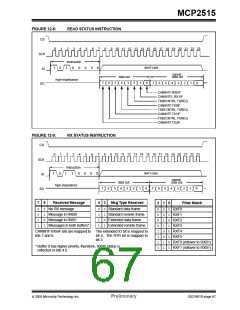
12.8 Read Status Instruction
The Read Status instruction allows single instruction
access to some of the often used status bits for
message reception and transmission.
The MCP2515 is selected by lowering the CS pin and
the read status command byte, shown in Figure 12-8,
is sent to the MCP2515. Once the command byte is
sent, the MCP2515 will return eight bits of data that
contain the status.
12.4 Read RX Buffer Instruction
The Read RX Buffer instruction (Figure 12-3) provides
a means to quickly address a receive buffer for reading.
This instruction reduces the SPI overhead by one byte,
the address byte. The command byte actually has four
possible values that determine the address pointer
location. Once the command byte is sent, the controller
clocks out the data at the address location the same as
If additional clocks are sent after the first eight bits are
transmitted, the MCP2515 will continue to output the
status bits as long as the CS pin is held low and clocks
are provided on SCK.
© 2005 Microchip Technology Inc.
Preliminary
DS21801D-page 63

 MICROCHIP [ MICROCHIP ]