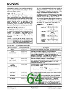
MCP2515
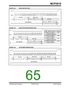
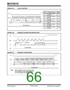
FIGURE 12-5:
LOAD TX BUFFER
a
b
c
Address Points to
Addr
CS
0
0
0
TX buffer 0, Start at
TXB0SIDH
0x31
0
1
2
3
4
5
6
7
8
9 10 11 12 13 14 15
0
0
0
1
1
0
1
1
0
0
1
0
1
0
1
TX buffer 0, Start at
TXB0D0
0x36
0x41
0x46
0x51
0x56
SCK
SI
TX buffer 1, Start at
TXB1SIDH
data in
instruction
TX buffer 1, Start at
TXB1D0
7
6
5
4
3
2
1
0
0
1
0
0
0
a
b
c
TX buffer 2, Start at
TXB2SIDH
high-impedance
SO
TX buffer 2, Start at
TXB2D0
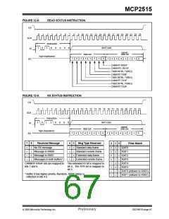
FIGURE 12-6:
REQUEST-TO-SEND (RTS) INSTRUCTION
CS
0
1
2
3
4
0
5
6
7
SCK
instruction
T1
0
1
0
0
T2
T0
SI
high-impedance
SO
FIGURE 12-7:
BIT MODIFY INSTRUCTION
CS
23 24 25 26 27 28 29 30 31
data byte
0
1 2 3 4 5 6 7 8 9 10 11 12 13 14 15 16 17 18 19 20 21 22
SCK
SI
mask byte
address byte
instruction
7
6 5 4 3 2 1 0
7 6 5 4 3 2 1 0
0
0 0 0 0 1 0 1 A7 6 5 4 3 2
1
A0
high-impedance
SO
Note:
Not all registers can be accessed with
this command. See the register map for a
list of the registers that apply.
DS21801D-page 66
Preliminary
© 2005 Microchip Technology Inc.

 MICROCHIP [ MICROCHIP ]