MCP2515
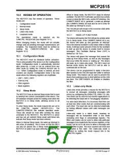
10.4 Loopback Mode
10.5 Normal Mode
Loopback mode will allow internal transmission of
messages from the transmit buffers to the receive
buffers without actually transmitting messages on the
CAN bus. This mode can be used in system
development and testing.
Normal mode is the standard operating mode of the
MCP2515. In this mode, the device actively monitors all
bus messages and generates acknowledge bits, error
frames, etc. This is also the only mode in which the
MCP2515 will transmit messages over the CAN bus.
In this mode, the ACK bit is ignored and the device will
allow incoming messages from itself just as if they were
coming from another node. The Loopback mode is a
silent mode, meaning no messages will be transmitted
while in this state (including error flags or acknowledge
signals). The TXCAN pin will be in a recessive state.
The filters and masks can be used to allow only
particular messages to be loaded into the receive
registers. The masks can be set to all zeros to provide
a mode that accepts all messages. The Loopback
mode is activated by setting the mode request bits in
the CANCTRL register.
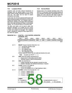
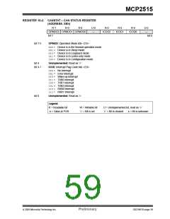
REGISTER 10-1: CANCTRL – CAN CONTROL REGISTER
(ADDRESS: XFh)
R/W-1
R/W-0
R/W-0
R/W-0
ABAT
R/W-0
OSM
R/W-1
R/W-1
R/W-1
REQOP2 REQOP1 REQOP0
bit 7
CLKEN CLKPRE1 CLKPRE0
bit 0
bit 7-5
REQOP: Request Operation Mode bits <2:0>
000= Set Normal Operation mode
001= Set Sleep mode
010= Set Loopback mode
011= Set Listen-only mode
100= Set Configuration mode
All other values for REQOP bits are invalid and should not be used
Note: On power-up, REQOP = b’111’
bit 4
ABAT: Abort All Pending Transmissions bit
1= Request abort of all pending transmit buffers
0= Terminate request to abort all transmissions
bit 3
OSM: One Shot Mode bit
1= Enabled. Message will only attempt to transmit one time
0= Disabled. Messages will reattempt transmission, if required
bit 2
CLKEN: CLKOUT Pin Enable bit
1= CLKOUT pin enabled
0= CLKOUT pin disabled (Pin is in high-impedance state)
bit 1-0
CLKPRE: CLKOUT Pin Prescaler bits <1:0>
00= FCLKOUT = System Clock/1
01= FCLKOUT = System Clock/2
10= FCLKOUT = System Clock/4
11= FCLKOUT = System Clock/8
Legend:
R = Readable bit
-n = Value at POR
W = Writable bit
U = Unimplemented bit, read as ‘0’
‘0’ = Bit is cleared x = Bit is unknown
‘1’ = Bit is set
DS21801D-page 58
Preliminary
© 2005 Microchip Technology Inc.

 MICROCHIP [ MICROCHIP ]