MCP2200
When the device starts normal operation (i.e., exits the
Reset condition), device operating parameters
(voltage, frequency, temperature, etc.) must be met to
ensure operation. If these conditions are not achieved,
the device must be held in Reset until the operating
conditions are met.
1.6.1.3
RxLED Pin Function (IN Message)
The ‘Rx’ in the pin name is in respect to the USB host.
The RxLED pin is an indicator for USB ‘IN’ messages.
This pin will either pulse low for a period of time
(configurable for ~100 ms or ~200 ms), or toggle to the
opposite state for every message received
(IN message) by the USB host. This allows the
application to count messages or provide a visual
indication of USB traffic.
1.9
Oscillator
The input clock must be 12 MHz to provide the proper
frequency for the USB module.
1.6.1.4
TxLED Pin Function (OUT Message)
USB full-speed is nominally 12 Mb/s. The clock input
accuracy is ±0.25% (2,500 ppm maximum).
The ‘Tx’ in the pin name is in respect to the USB host.
The TxLED pin is an indicator for USB ‘OUT’
messages.
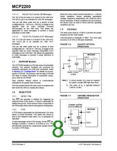
FIGURE 1-6:
QUARTZ CRYSTAL
OPERATION
This pin will either pulse low for a period of time
(configurable for ~100 ms or ~200 ms), or toggle to the
opposite state for every message transmitted (OUT
message) by the USB host. This allows the application
to count messages or provide a visual indication of
USB traffic.
MCP2200
OSC1
1.7
EEPROM Module
(2)
RF
The EEPROM module is a 256 byte array of nonvolatile
memory. The memory locations are accessed for
read/write operations via USB host commands. Refer
to Section 2.0 “Configuration” for details on access-
ing the EEPROM. The memory cells for data EEPROM
are rated to endure thousands of erase/write cycles,
up to 100K for EEPROM.
(1)
OSC2
RS
Quartz Crystal
12 MHz
Note 1: A series resistor (RS) may be required
Data retention without refresh is conservatively
estimated to be greater than 40 years.
for quartz crystals with high drive level.
2: The value of RF is typically between
2 M to 10 M..
The host should wait for the write cycle to complete and
then verify the write by reading the byte(s).
1.8
RESET/POR
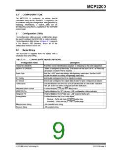
FIGURE 1-7:
CERAMIC RESONATOR
OPERATION
1.8.1
RESET PIN
The RST pin provides a method for triggering an
external Reset of the device. A Reset is generated by
holding the pin low. These devices have a noise filter in
the Reset path which detects and ignores small pulses.
Example: muRata
CSTCE12M0G15L
MCP2200
1.8.2
POR
OSC1
A POR pulse is generated on-chip whenever VDD rises
above a certain threshold. This allows the device to
start in the initialized state when VDD is adequate for
operation.
To take advantage of the POR circuitry, tie the RST pin
through a resistor (1 kOhm to 10 kOhm) to VDD. This
will eliminate external RC components usually needed
to create a POR delay.
OSC2
Resonator
12 MHz
DS22228B-page 8
2011 Microchip Technology Inc.

 MICROCHIP [ MICROCHIP ]