MCP201
2.3
AC Specifications
Electrical Characteristics:
Unless otherwise indicated, all limits are specified for:
VBAT = 6.0V to 18.0V
AC Specifications
TAMB = -40°C to +125°C
Symbol
Parameter
Min
Typical
Max
Units Conditions
Bus Interface
|dV/dt|
|dV/dt|
Slope Rising and Falling Edges
1.0
2.0
2.0
4.0
3.0
6.0
V/µs (40% to 60%), No Load
Slope Rising and Falling edges
ALTERNATE
V/µs (Note 1), No Load
tTRANSPD
tRECPD
Propagation Delay of Transmitter
Propagation Delay of Receiver
—
—
—
—
—
6.0
6.0
2.0
µs
µs
µs
tRECPD = max
(tRECPDR or tRECPDF
tRECSYM = max
)
tRECSYM
Symmetry of Propagation Delay of
Receiver Rising Edge with Respect
to Falling Edge
-2.0
tTRANSSYM Symmetry of Propagation Delay of
Transmitter Rising Edge with
-2.0
—
2.0
µs
tTRANSSYM = max
(tTRANSPDF - tRANSPDR
)
Respect to Falling Edge
Voltage Regulator
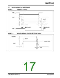
tBACTVE
tVEVR
tVREGPO
Bus Activity to Voltage Regulator
Enabled
10
—
—
—
50
—
40
200
2.5
µs
µs
Bus debounce time
Voltage Regulator Enabled to
Ready
(Note 2)
R
Voltage Regulator Enabled to
Ready after POR
ms
(Note 2) CLOAD = 25 nF
tCSOR
tCSPD
Chip Select to Operation Ready
Chip Select to Power-down
0
0
50
—
200
40
µs
µs
µs
(Note 2)
(Note 2) No CLOAD
tSHUTDOWN Short-Circuit to Shutdown
—
450
—
Characterized but not
tested
tSCREC
Short-Circuit Recovery Time
—
2.0
—
ms
Characterized but not
tested (Note 3)
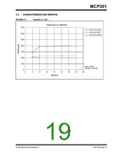
Note 1: The mode does not conform to LIN Bus specification version 1.3.
2: Time depends on external capacitance and load.
3: Internal current limited. 2.0 ms typical recovery time (RLBUS = 0Ω, TX = 0.4 VREG, VLBUS = VBAT, TAMB =
25C. Recovery time highly dependent on ambient temperature, package, and thermal resistance).
TABLE 2-1:
Sym
MCP201 THERMAL SPECIFICATIONS
Parameter
Min
Typical
Max
Units
Test Conditions
θRECOVERY Recovery Temperature
—
+135
—
°C
Characterized but not
tested
(junction temperature)
θSHUTDOWN Shutdown Temperature
—
—
+155
2.0
—
—
°C
Characterized but not
tested
(junction temperature)
tTHERM
Thermal Recovery Time
ms
Characterized but not
(after Fault condition removed)
tested (Note 1)
Note 1: Internal current limited. 2.0 ms typical recovery time (RLBUS = 0Ω, TX = 0.4 VREG, VLBUS = VBAT, TAMB =
25C. Recovery time highly dependent on ambient temperature, package, and thermal resistance).
DS21730F-page 16
© 2007 Microchip Technology Inc.

 MICROCHIP [ MICROCHIP ]