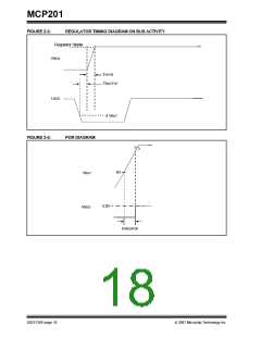
MCP201
2.2
DC Specifications
Electrical Characteristics:
Unless otherwise indicated, all limits are specified for:
VBAT = 6.0V to 18.0V
DC Specifications
TAMB = -40°C to +125°C
CLOADREG = 10 µF
Sym.
Parameter
Min.
Typ.
Max.
Units
Conditions
Power
IBATQ
VBAT Quiescent Operating
Current (voltage regulator
without load and transceiver)
—
0.45
1.0
mA IVREG = 0 mA, LIN bus pin
recessive, (Note 3)
IBAT
IDDQ
IVREG
VBAT Power-down Current
transceiver only
—
—
—
23
500
—
50
—
50
µA
µA
CS/WAKE = High, voltage
regulator disabled
VREG Quiescent Operating
Current
(Note 2)
VREG maximum output
current
mA (Note 4)
Microcontroller Interface
VIH
VIL
High-level Input Voltage
(TXD, FAULT/SLPS)
2.0
-0.3
-90
-150
3.0
-0.3
-10
5
—
—
—
—
—
—
—
—
—
—
VREG + 0.3
0.15 x VREG
+30
V
V
Low-level Input Voltage
(TXD, FAULT/SLPS)
IIHTXD
IILTXD
High-level Output Current
(TXD)
µA
µA
V
Input voltage = 4V
Low-level Output Current
(TXD)
-10
Input voltage = 1V (though
> 50 kΩ internal pull-up)
VIHCS/
WAKE
High-level Input Voltage
(CS/WAKE)
VBAT
Through an external current-
limiting resistor (10 kΩ)
VILCS/
WAKE
Low-level Input Voltage
(CS/WAKE)
1.0
V
IIHCS/
WAKE
High-level Input Current
(CS/WAKE)
+80
µA
µA
Input voltage = 4V (though
>100 kΩ internal pull-down)
IILCS/
WAKE
Low-level Input Current
(CS/WAKE)
30
Input voltage = 1V
IOH = -4 mA
VOHRXD High-level Output Voltage
(RXD)
0.8
VREG
—
VOLRXD Low-level Output Voltage
(RXD)
—
0.2 VREG
IOL = 4 mA
Note 1: Internal current limited. 2.0 ms typical recovery time (RLBUS = 0Ω, TX = 0.4 VREG, VLBUS = VBAT, TAMB =
25C. Recovery time highly dependent on ambient temperature, package and thermal resistance).
2: For design guidance only, not tested.
3: This current is at the VBAT pin.
4: The maximum power dissipation is a function of TJMAX, ΘJA and ambient temperature TA. The maximum
allowable power dissipation at an ambient temperature is PD = (TJMAX - TA)ΘJA. If this dissipation is
exceeded, the die temperature will rise above 150°C and the MCP201 will go into thermal shutdown.
DS21730F-page 14
© 2007 Microchip Technology Inc.

 MICROCHIP [ MICROCHIP ]