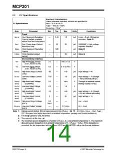
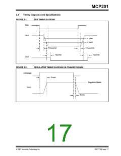
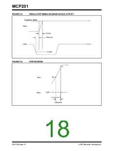
MCP201
2.2
DC Specifications (Continued)
Electrical Characteristics:
Unless otherwise indicated, all limits are specified for:
VBAT = 6.0V to 18.0V
DC Specifications
TAMB = -40°C to +125°C
CLOADREG = 10 µF
Sym.
Parameter
Min.
Typ.
Max.
Units
Conditions
Bus Interface
VIHLBUS High-level Input Voltage
(LBUS)
0.6 VBAT
-8
—
—
—
—
—
—
18
0.4 VBAT
0.1 VBAT
200
V
V
V
Recessive state
VILLBUS Low-level Input Voltage
(LBUS)
Dominant state
VIH - VIL
VHYS
IOL
IO
Input Hysteresis
0.05
VBAT
Low-level Output Current
(LBUS)
40
-20
mA Output voltage = 0.1 VBAT,
VBAT = 12V
High-level Output Current
(LBUS)
20
µA
VBUS ≥ VBAT, VLBUS < 40V
IP
Pull-up Current on Input
(LBUS)
-180
-60
µA
Approx. 30 kΩ internal pull-up
@ VIH = 0.7 VBAT
ISC
Short-circuit Current-Limit
50
—
—
200
—
mA (Note 1)
VOH
High-level Output Voltage
(LBUS)
0.8 VBAT
V
VOL
Low-level Output Voltage
(LBUS)
—
—
0.2 VBAT
V
Voltage Regulator
VREG
Output Voltage
4.75
4.4
—
—
5.25
5.25
V
V
0 mA > IOUT > 50 mA,
7.0V < VBAT < 18V
VREG1
Output Voltage
0 mA > IOUT > 50 mA,
6.0V < VBAT < 7.0V
ΔVREG1 Line Regulation
ΔVREG2 Load Regulation
—
—
10
10
50
50
mV IOUT = 1 mA, 7.0V < VBAT < 18V
mV 5 mA < IOUT < 50 mA,
VBAT = Constant
VN
Output Noise Voltage
—
—
—
400
4.0
µVRMS 1 VRMS @ 10 Hz - 100 kHz
VSD
Shutdown Voltage
(monitoring VREG)
3.5
V
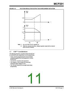
See Figure 1-4
VON
Input Voltage to Turn On
Output (monitoring VBAT)
5.5
—
6.0
V
Note 1: Internal current limited. 2.0 ms typical recovery time (RLBUS = 0Ω, TX = 0.4 VREG, VLBUS = VBAT, TAMB =
25C. Recovery time highly dependent on ambient temperature, package and thermal resistance).
2: For design guidance only, not tested.
3: This current is at the VBAT pin.
4: The maximum power dissipation is a function of TJMAX, ΘJA and ambient temperature TA. The maximum
allowable power dissipation at an ambient temperature is PD = (TJMAX - TA)ΘJA. If this dissipation is
exceeded, the die temperature will rise above 150°C and the MCP201 will go into thermal shutdown.
© 2007 Microchip Technology Inc.
DS21730F-page 15

 MICROCHIP [ MICROCHIP ]