HV9910B
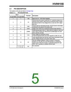
to control the IC. The VDD pin must be bypassed by a
low-ESR capacitor to provide a low impedance path for
the high frequency current of the output GATE driver.
3.0
APPLICATION INFORMATION
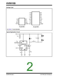
HV9910B is optimized to drive buck LED drivers using
open-loop, peak current mode control. This method of
control enables fairly accurate LED current control
without the need for high side current sensing or the
design of any closed loop controllers. The IC uses very
few external components and enables both Linear and
PWM-dimming of the LED current.
HV9910B can also be operated by supplying a voltage
at the VDD pin greater than the internally regulated
voltage. This will turn off the internal linear regulator of
the IC and the HV9910B will operate directly off the
voltage supplied at the VDD pin. Please note that this
external voltage at the VDD pin should not exceed 12V.
A resistor connected to the RT pin programs the fre-
quency of operation (or the off-time). The oscillator pro-
duces pulses at regular intervals. These pulses set the
SR flip-flop in the HV9910B which causes the GATE
driver to turn on. The same pulses also start the blank-
ing timer, which inhibits the reset input of the SR flip-
flop and prevent false turn-offs due to the turn-on spike.
When the FET turns on, the current through the induc-
tor starts ramping up. This current flows through the
external sense resistor RCS and produces a ramp volt-
age at the CS pin. The comparators are constantly
comparing the CS pin voltage to both the voltage at the
LD pin and the internal 250mV. Once the blanking timer
is complete, the output of these comparators is allowed
to reset the flip-flop. When the output of either one of
the two comparators goes high, the flip flop is reset and
the GATE output goes low. The GATE goes low until
the SR flip-flop is set by the oscillator. Assuming a 30%
ripple in the inductor, the current sense resistor RCS
can be set using:
Although the VIN pin of the HV9910B is rated up to
450V, the actual maximum voltage that can be applied
is limited by the power dissipation in the IC. For exam-
ple, if an 8-pin SOIC (junction to ambient thermal resis-
tance Rθ,j-a = 128°C/W) HV9910B draws about IIN
=
2.0mA from the VIN pin, and has a maximum allowable
temperature rise of the junction temperature limited to
about ∆T = 100°C, the maximum voltage at the VIN pin
would be:
T
-------------- ----- -------------------------- ------------
= 390V
1
100C
1
VINMAX
=
=
Rj – a IIN 128C W 2mA
In these cases, to operate the HV9910B from higher
input voltages, a Zener diode can be added in series
with the VIN pin to divert some of the power loss from
the HV9910B to the Zener diode. In the above exam-
ple, using a 100V Zener diode will allow the circuit to
easily work up to 450V.
0.25VorVLD
RCS = ------------------------------------
1.15 ILEDA
The input current drawn from the VIN pin is a sum of the
1.0mA current drawn by the internal circuit and the cur-
rent drawn by the GATE driver.The GATE driver
depends on the switching frequency and the GATE
charge of the external FET).
Constant frequency peak current mode control has an
inherent disadvantage – at duty cycles greater than
0.5, the control scheme goes into subharmonic oscilla-
tions. To prevent this, an artificial slope is typically
added to the current sense waveform. This slope com-
pensation scheme will affect the accuracy of the LED
current in the present form. However, a constant off-
time peak current control scheme does not have this
problem and can easily operate at duty cycles greater
then 0.5. This control scheme also gives inherent input
voltage rejection, making the LED current almost
insensitive to input voltage variations. However, this
scheme leads to variable frequency operation and the
frequency range depends greatly on the input and out-
put voltage variation. HV9910B makes it easy to switch
between the two modes of operation by changing one
connection (see Section 3.3 “Oscillator”).
IIN 1.0mA + Qg fs
In the above equation, fS is the switching frequency and
QG is the GATE charge of the external FET (which can
be obtained from the data sheet of the FET).
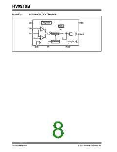
3.2
Current Sense
The current sense input of the HV9910B goes to the
non-inverting inputs of two comparators. The inverting
terminal of one comparator is tied to an internal 250mV
reference, whereas the inverting terminal of the other
comparator is connected to the LD pin. The outputs of
both these comparators are fed into an OR GATE and
the output of the OR GATE is fed into the reset pin of
the flip-flop. Thus, the comparator which has the lowest
voltage at the inverting terminal determines when the
GATE output is turned off.
3.1
Input Voltage Regulator
HV9910B can be powered directly from its VIN pin and
can work from 8.0 - 450VDC at its VIN pin. When a volt-
age is applied at the VIN pin, the HV9910B maintains a
constant 7.5V at the VDD pin. This voltage is used to
power the IC and any external resistor dividers needed
DS20005344A-page 6
2015 Microchip Technology Inc.

 MICROCHIP [ MICROCHIP ]