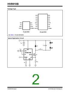
HV9910B
1
TABLE 1-1:
Symbol
ELECTRICAL CHARACTERISTICS (CONTINUED) (SHEET 2 OF 2)
Parameter
Note
Min
Typ
Max Units Conditions
Current Sense Comparator
225
213
250
250
275
287
-40°C < TA < +85°C
Current sense pull-in thresh-
old voltage
VCS,TH
-
mV
mV
TA < +125°C
Offset voltage for LD com-
parator
3
VOFFSET
-12
-
12
0 < TA < +85°C, VLD = VDD
,
-
150
215
280
VCS = VCS,TH + 50mV after
TBLANK
Current sense blanking
interval
TBLANK
ns
-40 < TA < +125°C, VLD = VDD
VCS = VCS,TH + 50mV after
TBLANK
,
-
-
145
-
215
80
315
150
VLD = VDD, VCS = VCS,TH
50mV after TBLANK
+
tDELAY
Delay to output
ns
Oscillator
-
-
20
80
25
30
RT = 1.00MΩ
RT = 226kΩ
fOSC
Oscillator frequency
kHz
100
120
Gate Driver
ISOURCE
ISINK
GATE sourcing current
GATE sinking current
GATE output rise time
GATE output fall time
-
-
-
-
165
-
-
mA VGATE = 0V, VDD = 7.5V
mA VGATE = VDD, VDD = 7.5V
165
-
-
tRISE
-
-
30
30
50
50
ns
ns
CGATE = 500pF, VDD = 7.5V
CGATE = 500pF, VDD = 7.5V
tFALL
1
2
3
4
Specifications are TA = 25°C, VIN = 15V unless otherwise noted.
Also limited by package-power dissipation limit; Whichever is lower.
Applies over the full operating ambient temperature range of -40°C < TA < +125°C.
For design guidance only
TABLE 1-2:
THERMAL RESISTANCE
Package
θja
8-Lead SOIC
16-Lead SOIC
101°C/W
83°C/W
DS20005344A-page 4
2015 Microchip Technology Inc.

 MICROCHIP [ MICROCHIP ]