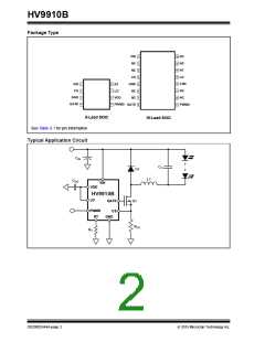
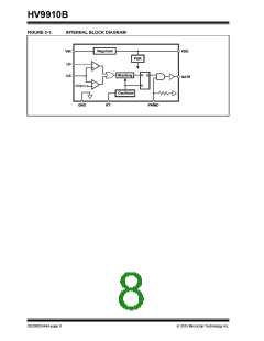
HV9910B
2.0
PIN DESCRIPTION
The locations of the pins are listed in Package Type.
TABLE 2-1: PIN DESCRIPTION
Pin #
8-Lead SOIC 16-Lead SOIC
Function
Description
1
1
VIN
Input of an 8.0 - 450V linear regulator.
Current sense pin used to sense the FET current by means of an
external sense resistor. When this pin exceeds the lower of either
the internal 250mV or the voltage at the LD pin, the GATE output
goes low.
2
4
CS
Ground return for all internal circuitry. This pin must be electrically
connected to the ground of the power train.
3
4
5
8
GND
GATE
Output GATE driver for an external N-channel power MOSFET.
PWM dimming input of the IC. When this pin is pulled to GND, the
GATE driver is turned off. When the pin is pulled high, the GATE
driver operates normally.
5
9
PWMD
Power supply for all internal circuits.
It must be bypassed with a low ESR capacitor to GND (≥0.1μF).
6
7
12
13
VDD
LD
Linear dimming input and sets the current sense threshold as long
as the voltage at the pin is less than 250mV (typ).
Sets the oscillator frequency. When a resistor is connected
between RT and GND, the HV9910B operates in constant fre-
quency mode. When the resistor is connected between RT and
GATE, the IC operates in constant off-time mode.
8
-
14
RT
NC
2, 3, 6, 7, 10,
11, 15, 16
No connection
2015 Microchip Technology Inc.
DS20005344A-page 5

 MICROCHIP [ MICROCHIP ]