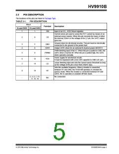
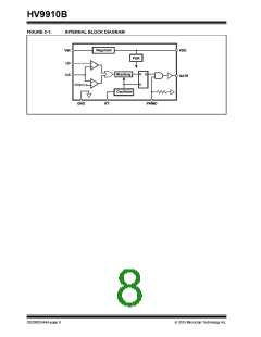
HV9910B
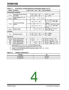
1.0
ELECTRICAL
CHARACTERISTICS
ABSOLUTE MAXIMUM RATINGS
VIN to GND......................................................-0.5V to +470V
V
DD to GND.......................................................................12V
CS, LD, PWMD, GATE, RT to GND.......-0.3V to (VDD + 0.3V)
Operating temperature..................................-40°C to +125°C
Storage temperature .....................................-65°C to +150°C
Continuous power dissipation (TA = +25°C)
8-lead SOIC...............................................630 mW
16-lead SOIC...........................................1300 mW
Note: Stresses above those listed under “Absolute Maximum
Ratings” may cause permanent damage to the device. This is
a stress rating only and functional operation of the device at
those or any other conditions, above those indicated in the
operational listings of this specification, is not implied. Expo-
sure to maximum rating conditions for extended periods may
affect device reliability.
1.1
ELECTRICAL SPECIFICATIONS
1
TABLE 1-1:
Symbol
ELECTRICAL CHARACTERISTICS (SHEET 1 OF 2)
Parameter
Note
Min
Typ
Max Units Conditions
Input
Input DC supply voltage
range2
3
3
VINDC
8.0
-
-
450
1.0
V
DC input voltage
Shut-down mode supply
current
IINSD
0.5
mA Pin PWMD to GND
Internal Regulator
VIN = 8.0V, IDD(ext) = 0, 500pF
VDD
Internally regulated voltage
-
-
7.25
0
7.5
7.75
1.0
V
V
at GATE; RT = 226kΩ, PWMD
= VDD
VIN = 8.0 - 450V, IDD(ext) = 0,
500pF at GATE; RT = 226kΩ,
PWMD = VDD
∆VDD, line Line regulation of VDD
∆VDD, load Load regulation of VDD
-
-
I
DD(ext) = 0 - 1.0mA, 500pF at
-
0
100
mV GATE; RT = 226kΩ, PWMD =
VDD
VDD undervoltage lockout
threshold
3
UVLO
6.45
-
6.7
6.95
-
V
VDD rising
DD falling
VDD undervoltage lockout
hysteresis
ꢀUVLO
-
500
mV
V
Current that the regulator
can supply before IC goes
into UVLO
4
IIN,MAX
5.0
-
-
mA VIN = 8.0V
PWM Dimming
VEN(lo) Pin PWMD input low voltage
VEN(hi)
3
3
-
-
-
0.8
-
V
V
VIN = 8.0 - 450V
Pin PWMD input high voltage
2.0
VIN = 8.0 - 450V
Pin PWMD pull-down resis-
tance at PWMD
REN
-
50
100
150
kΩ
VPWMD = 5.0V
2015 Microchip Technology Inc.
DS20005344A-page 3

 MICROCHIP [ MICROCHIP ]