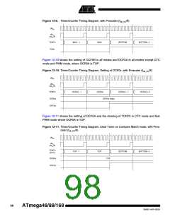
Figure 12-9. Timer/Counter Timing Diagram, with Prescaler (fclk_I/O/8)
clkI/O
clkTn
(clkI/O/8)
TCNTn
TOVn
MAX - 1
MAX
BOTTOM
BOTTOM + 1
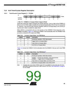
Figure 12-10 shows the setting of OCF0B in all modes and OCF0A in all modes except CTC
mode and PWM mode, where OCR0A is TOP.
Figure 12-10. Timer/Counter Timing Diagram, Setting of OCF0x, with Prescaler (fclk_I/O/8)
clkI/O
clkTn
(clkI/O/8)
TCNTn
OCRnx
OCFnx
OCRnx - 1
OCRnx
OCRnx + 1
OCRnx + 2
OCRnx Value
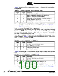
Figure 12-11 shows the setting of OCF0A and the clearing of TCNT0 in CTC mode and fast
PWM mode where OCR0A is TOP.
Figure 12-11. Timer/Counter Timing Diagram, Clear Timer on Compare Match mode, with Pres-
caler (fclk_I/O/8)
clkI/O
clkTn
(clkI/O/8)
TCNTn
(CTC)
TOP - 1
TOP
BOTTOM
BOTTOM + 1
OCRnx
TOP
OCFnx
98
ATmega48/88/168
2545E–AVR–02/05

 MICROCHIP [ MICROCHIP ]