ATmega48/88/168
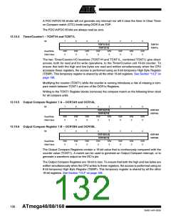
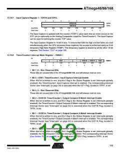
13.10.7 Input Capture Register 1 – ICR1H and ICR1L
Bit
7
6
5
4
3
2
1
0
ICR1[15:8]
ICR1[7:0]
ICR1H
ICR1L
Read/Write
Initial Value
R/W
0
R/W
0
R/W
0
R/W
0
R/W
0
R/W
0
R/W
0
R/W
0
The Input Capture is updated with the counter (TCNT1) value each time an event occurs on the
ICP1 pin (or optionally on the Analog Comparator output for Timer/Counter1). The Input Capture
can be used for defining the counter TOP value.
The Input Capture Register is 16-bit in size. To ensure that both the high and low bytes are read
simultaneously when the CPU accesses these registers, the access is performed using an 8-bit
temporary High Byte Register (TEMP). This temporary register is shared by all the other 16-bit
registers. See Section “13.2” on page 108.
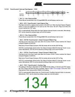
13.10.8 Timer/Counter1 Interrupt Mask Register – TIMSK1
Bit
7
6
5
4
–
3
–
2
OCIE1B
R/W
0
1
OCIE1A
R/W
0
0
TOIE1
R/W
0
–
–
ICIE1
TIMSK1
Read/Write
Initial Value
R
0
R
0
R/W
0
R
0
R
0
• Bit 7, 6 – Res: Reserved Bits
These bits are unused bits in the ATmega48/88/168, and will always read as zero.
• Bit 5 – ICIE1: Timer/Counter1, Input Capture Interrupt Enable
When this bit is written to one, and the I-flag in the Status Register is set (interrupts globally
enabled), the Timer/Counter1 Input Capture interrupt is enabled. The corresponding Interrupt
Vector (see “Interrupts” on page 54) is executed when the ICF1 Flag, located in TIFR1, is set.
• Bit 4, 3 – Res: Reserved Bits
These bits are unused bits in the ATmega48/88/168, and will always read as zero.
• Bit 2 – OCIE1B: Timer/Counter1, Output Compare B Match Interrupt Enable
When this bit is written to one, and the I-flag in the Status Register is set (interrupts globally
enabled), the Timer/Counter1 Output Compare B Match interrupt is enabled. The corresponding
Interrupt Vector (see “Interrupts” on page 54) is executed when the OCF1B Flag, located in
TIFR1, is set.
• Bit 1 – OCIE1A: Timer/Counter1, Output Compare A Match Interrupt Enable
When this bit is written to one, and the I-flag in the Status Register is set (interrupts globally
enabled), the Timer/Counter1 Output Compare A Match interrupt is enabled. The corresponding
Interrupt Vector (see “Interrupts” on page 54) is executed when the OCF1A Flag, located in
TIFR1, is set.
• Bit 0 – TOIE1: Timer/Counter1, Overflow Interrupt Enable
When this bit is written to one, and the I-flag in the Status Register is set (interrupts globally
enabled), the Timer/Counter1 Overflow interrupt is enabled. The corresponding Interrupt Vector
(See Section “8.2” on page 49.) is executed when the TOV1 Flag, located in TIFR1, is set.
133
2545E–AVR–02/05

 MICROCHIP [ MICROCHIP ]