93LC46A/B
3.8
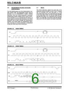
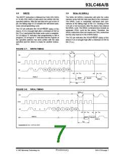
WRITE
3.9
Write All (WRAL)
The WRITE instruction is followed by 8 bits (93LC46A)
or 16 bits (93LC46B) of data which are written into the
specified address. After the last data bit is put on the DI
pin, the falling edge of CS initiates the self-timed auto-
erase and programming cycle.
The Write All (WRAL) instruction will write the entire
memory array with the data specified in the command.
The WRAL cycle is completely self-timed and com-
mences at the falling edge of the CS. Clocking of the
CLK pin is not necessary after the device has entered
the WRAL cycle.The WRAL command does include an
automatic ERAL cycle for the device. Therefore, the
WRAL instruction does not require an ERAL instruction
but the chip must be in the EWEN status.
The DO pin indicates the READY/BUSY status of the
device, if CS is brought high after a minimum of 250 ns
low (TCSL) and before the entire write cycle is complete.
DO at logical “0” indicates that programming is still in
progress. DO at logical “1” indicates that the register at
the specified address has been written with the data
specified and the device is ready for another instruc-
tion.
The DO pin indicates the READY/BUSY status of the
device if CS is brought high after a minimum of 250 ns
low (TCSL).
FIGURE 3-7: WRITE TIMING
TCSL
CS
CLK
0
1
1
An
A0
Dx
D0
•••
•••
DI
TSV
TCZ
HIGH-Z
BUSY
READY
DO
HIGH-Z
Twc
FIGURE 3-8: WRAL TIMING
TCSL
CS
CLK
0
0
1
X
1
0
•••
Dx
•••
DI
X
D0
TSV
TCZ
HIGH-Z
BUSY
READY
DO
HIGH-Z
TWL
Guaranteed at Vcc = 4.5V to +6.0V.
1997 Microchip Technology Inc.
Preliminary
DS21173D-page 7

 MICROCHIP [ MICROCHIP ]