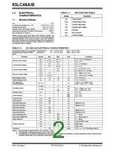
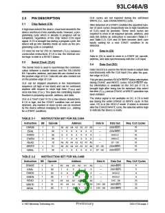
93LC46A/B
3.6
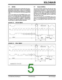
ERASE/WRITE Disable and Enable
(EWDS/EWEN)
3.7
READ
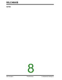
The READ instruction outputs the serial data of the
addressed memory location on the DO pin. A dummy
zero bit precedes the 8-bit (93LC46A) or 16-bit
(93LC46B) output string.The output data bits will toggle
on the rising edge of the CLK and are stable after the
specified time delay (TPD). Sequential read is possible
when CS is held high. The memory data will automati-
cally cycle to the next register and output sequentially.
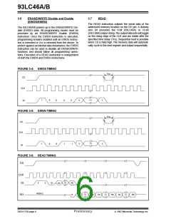
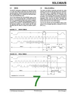
The 93LC46A/B powers up in the ERASE/WRITE Dis-
able (EWDS) state. All programming modes must be
preceded by an ERASE/WRITE Enable (EWEN)
instruction. Once the EWEN instruction is executed,
programming remains enabled until an EWDS instruc-
tion is executed or Vcc is removed from the device. To
protect against accidental data disturbance, the EWDS
instruction can be used to disable all ERASE/WRITE
functions and should follow all programming opera-
tions. Execution of a READ instruction is independent
of both the EWEN and EWDS instructions.
FIGURE 3-4: EWDS TIMING
TCSL
CS
CLK
•••
X
1
0
0
0
0
X
DI
FIGURE 3-5: EWEN TIMING
TCSL
CS
CLK
•••
1
0
0
1
1
X
X
DI
FIGURE 3-6: READ TIMING
CS
CLK
•••
A0
0
DI
An
1
1
0
HIGH-Z
DO
Dx
D0
Dx
D0
Dx
D0
•••
•••
•••
DS21173D-page 6
Preliminary
1997 Microchip Technology Inc.

 MICROCHIP [ MICROCHIP ]