93LC46A/B
3.4
ERASE
3.5
Erase All (ERAL)
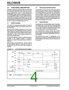
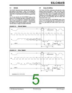
The ERASE instruction forces all data bits of the spec-
ified address to the logical “1” state. CS is brought low
following the loading of the last address bit. This falling
edge of the CS pin initiates the self-timed programming
cycle.
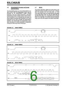
The Erase All (ERAL) instruction will erase the entire
memory array to the logical “1” state. The ERAL cycle
is identical to the ERASE cycle, except for the different
opcode. The ERAL cycle is completely self-timed and
commences at the falling edge of the CS. Clocking of
the CLK pin is not necessary after the device has
entered the ERAL cycle.
The DO pin indicates the READY/BUSY status of the
device if CS is brought high after a minimum of 250 ns
low (TCSL). DO at logical “0” indicates that program-
ming is still in progress. DO at logical “1” indicates that
the register at the specified address has been erased
and the device is ready for another instruction.
The DO pin indicates the READY/BUSY status of the
device, if CS is brought high after a minimum of 250 ns
low (TCSL) and before the entire ERAL cycle is com-
plete.
FIGURE 3-2: ERASE TIMING
TCSL
CS
CHECK STATUS
CLK
1
1
AN
AN-1 AN-2
A0
•••
DI
1
TSV
TCZ
HIGH-Z
BUSY
READY
DO
HIGH-Z
TWC
FIGURE 3-3: ERAL TIMING
TCSL
CS
CHECK STATUS
CLK
1
0
0
1
0
X
X
DI
•••
TSV
TCZ
HIGH-Z
BUSY
READY
DO
HIGH-Z
TEC
Guaranteed at Vcc = 4.5V to +6.0V.
1997 Microchip Technology Inc.
Preliminary
DS21173D-page 5

 MICROCHIP [ MICROCHIP ]