25AA512/25LC512
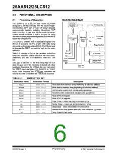
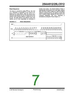
provide clock pulses. The internal Address Pointer is
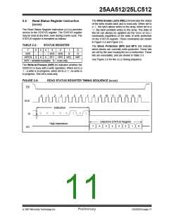
automatically incremented to the next higher address
after each byte of data is shifted out. When the highest
address is reached (FFFFh), the address counter rolls
over to address 0000h allowing the read cycle to be
continued indefinitely. The READ instruction is
terminated by raising the CS pin (Figure 2-1).
Read Sequence
The device is selected by pulling CS low. The 8-bit
READ instruction is transmitted to the 25XX512 fol-
lowed by the 16-bit address. After the correct READ
instruction and address are sent, the data stored in the
memory at the selected address is shifted out on the
SO pin. The data stored in the memory at the next
address can be read sequentially by continuing to
FIGURE 2-1:
READ SEQUENCE
CS
0
1
2
3
4
5
6
7
8
9 10 11
21 22 23 24 25 26 27 28 29 30 31
SCK
Instruction
16-bit Address
15 14 13 12
0
0
0
0
0
0
1
1
2
1
0
SI
Data Out
High-Impedance
7
6
5
4
3
2
1
0
SO
© 2007 Microchip Technology Inc.
Preliminary
DS22021B-page 7

 MICROCHIP [ MICROCHIP ]