25AA512/25LC512
2.0
2.1
FUNCTIONAL DESCRIPTION
Principles of Operation
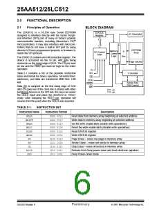
BLOCK DIAGRAM
The 25XX512 is a 65,536 byte Serial EEPROM
designed to interface directly with the Serial Periph-
eral Interface (SPI) port of many of today’s popular
microcontroller families, including Microchip’s PIC®
microcontrollers. It may also interface with microcon-
trollers that do not have a built-in SPI port by using
discrete I/O lines programmed properly in firmware to
match the SPI protocol.
STATUS
Register
HV Generator
EEPROM
Array
Memory
Control
Logic
X
I/O Control
Logic
Dec
The 25XX512 contains an 8-bit instruction register. The
device is accessed via the SI pin, with data being
clocked in on the rising edge of SCK. The CS pin must
be low and the HOLD pin must be high for the entire
operation.
Page Latches
Y Decoder
SI
SO
Table 2-1 contains a list of the possible instruction
bytes and format for device operation. All instructions,
addresses, and data are transferred MSB first, LSB
last.
CS
SCK
Sense Amp.
R/W Control
HOLD
WP
Data (SI) is sampled on the first rising edge of SCK
after CS goes low. If the clock line is shared with other
peripheral devices on the SPI bus, the user can assert
the HOLD input and place the 25XX512 in ‘HOLD’
mode. After releasing the HOLD pin, operation will
resume from the point when the HOLD was asserted.
VCC
VSS
TABLE 2-1:
INSTRUCTION SET
Instruction Name
Instruction Format
Description
READ
WRITE
WREN
WRDI
RDSR
WRSR
PE
0000 0011
0000 0010
0000 0110
0000 0100
0000 0101
0000 0001
0100 0010
1101 1000
1100 0111
1010 1011
1011 1001
Read data from memory array beginning at selected address
Write data to memory array beginning at selected address
Set the write enable latch (enable write operations)
Reset the write enable latch (disable write operations)
Read STATUS register
Write STATUS register
Page Erase – erase one page in memory array
Sector Erase – erase one sector in memory array
Chip Erase – erase all sectors in memory array
Release from Deep power-down and read electronic signature
Deep Power-Down mode
SE
CE
RDID
DPD
DS22021B-page 6
Preliminary
© 2007 Microchip Technology Inc.

 MICROCHIP [ MICROCHIP ]