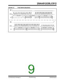
25AA512/25LC512
1.0
ELECTRICAL CHARACTERISTICS
(†)
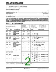
Absolute Maximum Ratings
VCC.............................................................................................................................................................................6.5V
All inputs and outputs w.r.t. VSS ......................................................................................................... -0.6V to VCC +1.0V
Storage temperature .................................................................................................................................-65°C to 150°C
Ambient temperature under bias...............................................................................................................-40°C to 125°C
ESD protection on all pins..........................................................................................................................................4 kV
† NOTICE: Stresses above those listed under “Absolute Maximum Ratings” may cause permanent damage to the
device. This is a stress rating only and functional operation of the device at those or any other conditions above those
indicated in the operational listings of this specification is not implied. Exposure to maximum rating conditions for an
extended period of time may affect device reliability.
TABLE 1-1:
DC CHARACTERISTICS
Industrial (I):
Industrial (I):
Automotive (E):
TA = 0°C to +85°C
TA = -40°C to +85°C
TA = -40°C to +125°C
VCC = 1.8V to 5.5V
VCC = 2.0V to 5.5V
VCC = 2.5V to 5.5V
DC CHARACTERISTICS
Param.
Sym.
Characteristic
Min.
Max.
VCC +1
Units
Test Conditions
No.
D001
VIH1
High-level input
voltage
.7 VCC
V
D002
D003
D004
D005
D006
VIL1
VIL2
VOL
VOL
VOH
Low-level input
voltage
-0.3
-0.3
0.3 VCC
0.2 VCC
0.4
V
V
V
V
V
VCC ≥ 2.7V
VCC < 2.7V
Low-level output
voltage
—
IOL = 2.1 mA
—
0.2
IOL = 1.0 mA, VCC < 2.5V
IOH = -400 μA
High-level output
voltage
VCC -0.5
—
D007
D008
ILI
Input leakage current
—
—
±1
±1
μA
μA
CS = VCC, VIN = VSS TO VCC
CS = VCC, VOUT = VSS TO VCC
ILO
Output leakage
current
D009
D010
CINT
Internal capacitance
(all inputs and
outputs)
—
7
pF
TA = 25°C, CLK = 1.0 MHz,
VCC = 5.0V (Note)
ICC Read
—
—
10
5
mA
mA
VCC = 5.5V; FCLK = 20.0 MHz;
SO = Open
VCC = 2.5V; FCLK = 10.0 MHz;
SO = Open
Operating current
D011
D012
ICC Write
ICCS
—
—
7
5
mA
mA
VCC = 5.5V
VCC = 2.5V
—
—
20
μA
CS = VCC = 5.5V, Inputs tied to VCC or
VSS, 125°C
Standby current
10
μA
CS = VCC = 5.5V, Inputs tied to VCC or
VSS, 85°C
D13
ICCSPD
Deep power-down
current
—
2
1
μA
μA
CS = VCC = 2.5V, Inputs tied to VCC or
VSS, 125°C
CS = VCC = 2.5V, Inputs tied to VCC or
VSS, 85°C
Note:
This parameter is periodically sampled and not 100% tested.
DS22021B-page 2
Preliminary
© 2007 Microchip Technology Inc.

 MICROCHIP [ MICROCHIP ]