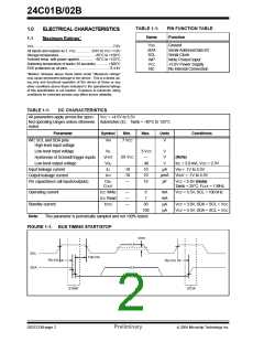
24C01B/02B
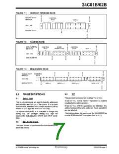
FIGURE 7-1: CURRENT ADDRESS READ
S
T
BUS ACTIVITY
CONTROL
S
T
O
P
A
R
T
MASTER
BYTE
DATA n
SDA LINE
S
P
A
C
K
N
O
BUS ACTIVITY
A
C
K
FIGURE 7-2: RANDOM READ
S
T
A
R
T
S
T
A
R
T
S
T
CONTROL
BYTE
WORD
ADDRESS (n)
CONTROL
BYTE
BUS ACTIVITY
MASTER
DATA n
O
P
P
S
S
SDA LINE
A
C
K
A
C
K
A
C
K
N
O
BUS ACTIVITY
A
C
K
FIGURE 7-3: SEQUENTIAL READ
S
A
C
K
A
C
K
A
C
K
T
CONTROL
BYTE
BUS ACTIVITY
MASTER
O
P
SDA LINE
P
A
C
K
N
O
BUS ACTIVITY
DATA n
DATA n + 1
DATA n + 2
DATA n + X
A
C
K
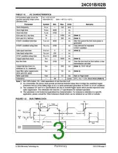
8.3
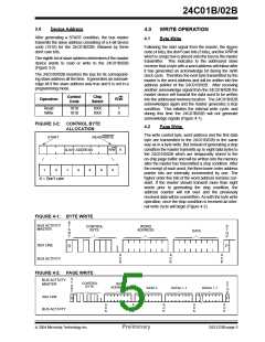
WP
8.0
PIN DESCRIPTIONS
This pin must be connected to either VSS or VCC.
8.1
Serial Data
If tied to VSS, normal memory operation is enabled
(read/write the entire memory).
This is a bi-directional pin used to transfer addresses
and data into and data out of the device. It is an open
drain terminal, therefore the SDA bus requires a pull-up
resistor to VCC (typically 10 K¾ for 100 kHz).
If tied to VCC, WRITE operations are inhibited. The
entire memory will be write-protected. Read operations
are not affected.
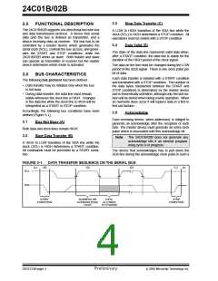
For normal data transfer SDA is allowed to change only
during SCL low. Changes during SCL high are
reserved for indicating the START and STOP condi-
tions.
This feature allows the user to use the 24C01B/02B as
a serial ROM when WP is enabled (tied to VCC).
8.2
SCL Serial Clock
This input is used to synchronize the data transfer from
and to the device.
2004 Microchip Technology Inc.
Preliminary
DS21233B-page 7

 MICROCHIP [ MICROCHIP ]