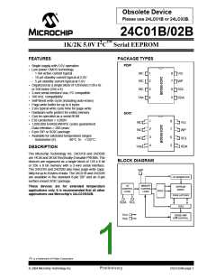
24C01B/02B
3.6
Device Address
4.0
WRITE OPERATION
After generating a START condition, the bus master
transmits the slave address consisting of a 4-bit device
code (1010) for the 24C01B/02B, followed by three
don't care bits.
4.1
Byte Write
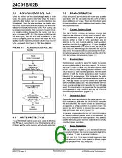
Following the start signal from the master, the device
code (4 bits), the don't care bits (3 bits), and the R/W bit
which is a logic low is placed onto the bus by the master
transmitter. This indicates to the addressed slave
receiver that a byte with a word address will follow after
it has generated an acknowledge bit during the ninth
clock cycle. Therefore the next byte transmitted by the
master is the word address and will be written into the
address pointer of the 24C01B/02B. After receiving
another acknowledge signal from the 24C01B/02B the
master device will transmit the data word to be written
into the addressed memory location. The 24C01B/02B
acknowledges again and the master generates a stop
condition. This initiates the internal write cycle, and
during this time the 24C01B/02B will not generate
acknowledge signals (Figure 4-1).
The eighth bit of slave address determines if the master
device wants to read or write to the 24C01B/02B
(Figure 3-2).
The 24C01B/02B monitors the bus for its correspond-
ing slave address all the time. It generates an acknowl-
edge bit if the slave address was true and it is not in a
programming mode.
Control
Code
Chip
Select
Operation
R/W
Read
Write
1010
1010
XXX
XXX
1
0
FIGURE 3-2: CONTROL BYTE
ALLOCATION
4.2
Page Write
The write control byte, word address and the first data
byte are transmitted to the 24C01B/02B in the same
way as in a byte write. But instead of generating a stop
condition the master transmits up to eight data bytes to
the 24C01B/02B which are temporarily stored in the
on-chip page buffer and will be written into the memory
after the master has transmitted a stop condition. After
the receipt of each word, the three lower order address
pointer bits are internally incremented by one. The
higher order five bits of the word address remains con-
stant. If the master should transmit more than eight
words prior to generating the stop condition, the
address counter will roll over and the previously
received data will be overwritten. As with the byte write
operation, once the stop condition is received an inter-
nal write cycle will begin (Figure 4-2).
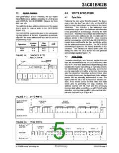
START
READ/WRITE
R/W
X
A
SLAVE ADDRESS
1
0
1
0
X
X
X = Don’t care
FIGURE 4-1: BYTE WRITE
S
BUS ACTIVITY
MASTER
T
A
R
T
S
T
O
P
CONTROL
BYTE
WORD
ADDRESS
DATA
SDA LINE
S
P
A
C
K
A
C
K
A
C
K
BUS ACTIVITY
FIGURE 4-2: PAGE WRITE
S
BUS ACTIVITY
MASTER
T
S
T
O
P
CONTROL
BYTE
WORD
ADDRESS (n)
A
R
T
DATA n
DATAn + 1
DATAn + 7
SDA LINE
S
P
A
C
K
A
C
K
A
C
K
A
C
K
A
C
K
BUS ACTIVITY
2004 Microchip Technology Inc.
Preliminary
DS21233B-page 5

 MICROCHIP [ MICROCHIP ]