24C01B/02B
5.0
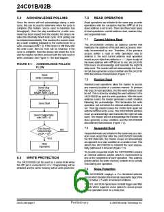
ACKNOWLEDGE POLLING
7.0
READ OPERATION
Since the device will not acknowledge during a write
cycle, this can be used to determine when the cycle is
complete (this feature can be used to maximize bus
throughput). Once the stop condition for a write com-
mand has been issued from the master, the device ini-
tiates the internally timed write cycle. ACK polling can
be initiated immediately. This involves the master send-
ing a start condition followed by the control byte for a
write command (R/W = 0). If the device is still busy with
the write cycle, then no ACK will be returned. If the
cycle is complete, then the device will return the ACK
and the master can then proceed with the next read or
write command. See Figure 5-1 for flow diagram.
Read operations are initiated in the same way as write
operations with the exception that the R/W bit of the
slave address is set to one. There are three basic types
of read operations: current address read, random read,
and sequential read.
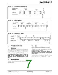
7.1
Current Address Read
The 24C01B/02B contains an address counter that
maintains the address of the last word accessed, inter-
nally incremented by one. Therefore, if the previous
access (either a read or write operation) was to
address n, the next current address read operation
would access data from address n + 1. Upon receipt of
the slave address with R/W bit set to one, the 24C01B/
02B issues an acknowledge and transmits the eight bit
data word. The master will not acknowledge the trans-
fer but does generate a stop condition and the 24C01B/
02B discontinues transmission (Figure 7-1).
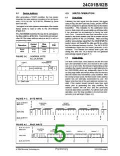
FIGURE 5-1: ACKNOWLEDGE POLLING
FLOW
Send
Write Command
7.2
Random Read
Random read operations allow the master to access
any memory location in a random manner. To perform
this type of read operation, first the word address must
be set. This is done by sending the word address to the
24C01B/02B as part of a write operation. After the word
address is sent, the master generates a start condition
following the acknowledge. This terminates the write
operation, but not before the internal address pointer is
set. Then the master issues the control byte again but
with the R/W bit set to a one. The 24C01B/02B will then
issue an acknowledge and transmits the eight bit data
word. The master will not acknowledge the transfer but
does generate a stop condition and the 24C01B/02B
discontinues transmission (Figure 7-2).
Send Stop
Condition to
Initiate Write Cycle
Send Start
Send Control Byte
with R/W = 0
7.3
Sequential Read
Did Device
NO
Acknowledge
Sequential reads are initiated in the same way as a ran-
dom read except that after the 24C01B/02B transmits
the first data byte, the master issues an acknowledge
as opposed to a stop condition in a random read. This
directs the 24C01B/02B to transmit the next sequen-
tially addressed 8-bit word (Figure 7-3).
(ACK = 0)?
YES
Next
Operation
To provide sequential reads the 24C01B/02B contains
an internal address pointer which is incremented by
one at the completion of each operation. This address
pointer allows the entire memory contents to be serially
read during one operation.
6.0
WRITE PROTECTION
The 24C01B/02B can be used as a serial ROM when
the WP pin is connected to VCC. Programming will be
inhibited and the entire memory will be write-protected.
7.4
Noise Protection
The 24C01B/02B employs a VCC threshold detector
circuit which disables the internal erase/write logic if the
VCC is below 1.5 volts at nominal conditions.
The SCL and SDA inputs have Schmitt trigger and filter
circuits which suppress noise spikes to assure proper
device operation even on a noisy bus.
DS21233B-page 6
Preliminary
2004 Microchip Technology Inc.

 MICROCHIP [ MICROCHIP ]