24C01B/02B
TABLE 1-2:
AC CHARACTERISTICS
All Parameters apply across the
specified operating ranges unless
otherwise noted
Vcc = 4.5V to 5.5V
Automotive (E):
Tamb = -40°C to +125°C,
Parameter
Symbol
Min.
Max.
Units
Remarks
Clock frequency
FCLK
THIGH
TLOW
TR
—
4000
4700
—
100
—
kHz
ns
Clock high time
Clock low time
—
ns
SDA and SCL rise time
SDA and SCL fall time
START condition hold time
1000
300
—
ns
(Note 1)
(Note 1)
TF
—
ns
THD:STA
4000
ns
After this period the first clock pulse is
generated
START condition setup time
TSU:STA
4700
—
ns
Only relevant for repeated
START condition
Data input hold time
Data input setup time
STOP condition setup time
Output valid from clock
Bus free time
THD:DAT
TSU:DAT
TSU:STO
TAA
0
—
—
ns
ns
ns
ns
ns
(Note 2)
(Note 2)
250
4000
—
—
3500
—
TBUF
4700
Time the bus must be free before a new
transmission can start
Output fall time from VIH
minimum to VIL maximum
TOF
TSP
—
—
250
50
ns
ns
(Note 1), CB ð 100 pF
Input filter spike suppression
(SDA and SCL pins)
(Note 3)
Write cycle time
Endurance
TWR
—
—
10
—
ms
Byte or Page mode
1M
cycles 25°C, Vcc = 5.0V, Block Mode (Note 4)
Note 1: Not 100% tested. CB = total capacitance of one bus line in pF.
2: As a transmitter, the device must provide an internal minimum delay time to bridge the undefined region
(minimum 300 ns) of the falling edge of SCL to avoid unintended generation of START or STOP conditions.
3: The combined TSP and VHYS specifications are due to Schmitt trigger inputs which provide improved noise
spike suppression. This eliminates the need for a TI specification for standard operation.
4: This parameter is not tested but guaranteed by characterization. For endurance estimates in a specific
application, please consult the Total Endurance Model which can be obtained on our BBS or website.
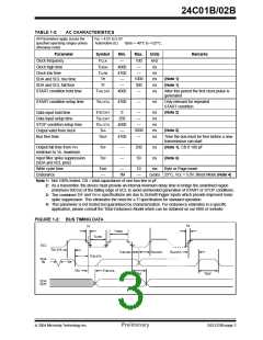
FIGURE 1-2: BUS TIMING DATA
TR
TF
THIGH
TLOW
SCL
TSU:STA
THD:DAT
TSU:DAT
TSU:STO
THD:STA
SDA
IN
TSP
TAA
THD:STA
TAA
TBUF
SDA
OUT
2004 Microchip Technology Inc.
Preliminary
DS21233B-page 3

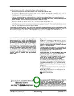
 MICROCHIP [ MICROCHIP ]