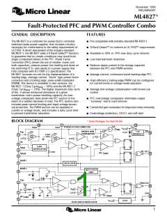
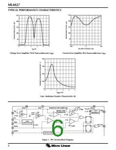
ML4827
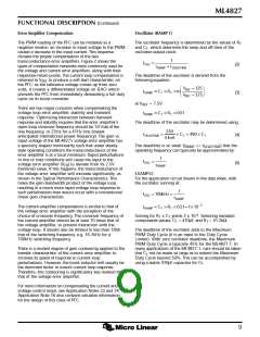
PIN CONFIGURATION
ML4827
16-Pin PDIP (P16)
16-Pin Wide SOIC (S16W)
IEAO
1
2
3
4
5
6
7
8
16 VEAO
I
15
14
13
V
V
V
AC
FB
I
SENSE
REF
CC
V
RMS
SS
12 PFC OUT
11 PWM OUT
10 GND
V
DC
RAMP 1
RAMP 2
9
DC I
LIMIT
TOP VIEW
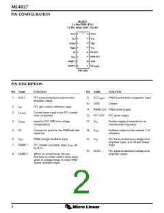
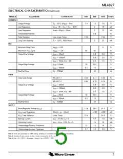
PIN DESCRIPTION
PIN NAME
FUNCTION
PIN NAME
FUNCTION
1
IEAO
PFC transconductance current error
amplifier output
9
DC I
GND
PWM current limit comparator input
Ground
LIMIT
10
11
12
13
2
3
I
AC
PFC gain control reference input
PWM OUT PWM driver output
I
Current sense input to the PFC current
limit comparator
SENSE
PFC OUT
PFC driver output
4
5
V
RMS
Input for PFC RMS line voltage
compensation
V
CC
Positive supply (connected to an
internal shunt regulator)
SS
Connection point for the PWM soft start
capacitor
14
15
V
V
Buffered output for the internal 7.5V
reference
REF
6
7
V
DC
PWM voltage feedback input
PFC transconductance voltage error
amplifier input, and TriFault Detect
input
FB
RAMP 1
RAMP 2
PFC (master) oscillator input; f
set
OSC
by R C
T
T
16
VEAO
PFC transconductance voltage error
amplifier output
8
When in current mode, this pin
functions as as the current sense input;
when in voltage mode, it is the PWM
(slave) oscillator input.
2

 MICRO-LINEAR [ MICRO LINEAR CORPORATION ]