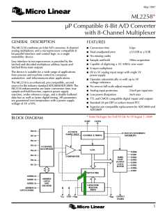
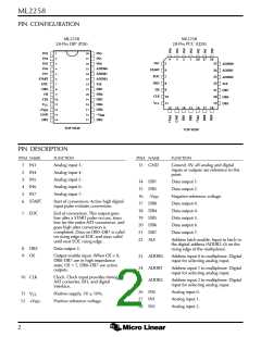
ML2258
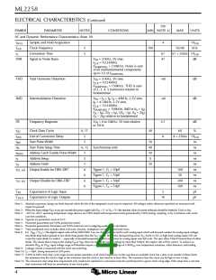
ELECTRICAL CHARACTERISTICS (Continued)
TYP
SYMBOL
PARAMETER
NOTES
CONDITIONS
MIN (NOTE 4)
MAX
UNITS
AC and Dynamic Performance Characteristics (Note 10)
tACQ
fCLK
tC
Sample and Hold Acquisition
Clock Frequency
4
1/fCLK
kHz
5
5
100
67
10240
Conversion Time
67 + 250ns 1/fCLK
dB
SNR
Signal to Noise Ratio
VIN = 51kHz, 5V sine.
fCLK = 10.24MHz
47
(fSAMPLING > 150kHz). Noise is sum
of all nonfundamental components
up to 1/2 of fSAMPLING
THD
IMD
Total Harmonic Distortion
Intermodulation Distortion
VIN = 51kHz, 5V sine.
fCLK = 10.24MHz
(fSAMPLING > 150kHz). THD is sum
of 2, 3, 4, 5 harmonics relative to
fundamental
–60
–60
dB
dB
V
IN = fA + fB. fA = 49kHz, 2.5V sine.
fB = 47.8kHz, 2.5V sine,
fCLK = 10.24MHz
(fSAMPLING > 150kHz). IMD is (fA + fB),
(fA – fB), (2fA + fB), (2fA – fB), (fA + 2fB),
(fA – 2fB) relative to fundamental
FR
Frequency Response
V
IN = 0 to 50kHz. 5V sine relative
0.1
dB
to 1kHz
tDC
tEOC
tWS
tSS
Clock Duty Cycle
6, 11
40
60
%
End of Conversion Delay
Start Pulse Width
5
8
8 + 250ns 1/fCLK
5
50
40
50
0
ns
ns
ns
ns
ns
Start Pulse Setup Time
Address Latch Enable Pulse Width
Address Setup
6, 12
Synchronous only
tWALE
tS
5
5
5
6
6
6
6
tH
Address Hold
50
tH1, H0 Output Enable for DB0–DB7
Figure 1, CL = 50pF
Figure 1, CL = 10pF
Figure 1, CL = 50pF
Figure 1, CL = 10pF
100
50
ns
ns
ns
ns
pF
pF
t1H, 0H Output Disable for DB0–DB7
200
100
CIN
Capacitance of Logic Input
5
COUT
Capacitance of Logic Outputs
10
Note 1: Absolute maximum ratings are limits beyond which the life of the integrated circuit may be impaired. All voltages unless otherwise specified are measured with
respect to ground.
Note 2: When the input voltage (VIN) at any pin exceeds the power supply rails (VIN < V– or VIN > V+) the absolute value of current at that pin should be limited to 25mA or less.
Note 3: –40°C to +85°C operating temperature range devices are 100% tested with temperature limits guaranteed by 100% testing, sampling, or by correlation with worst-
case test conditions.
Note 4: Typicals are parametric norm at 25°C.
Note 5: Parameter guaranteed and 100% production tested.
Note 6: Parameter guaranteed. Parameters not 100% tested are not in outgoing quality level calculation.
Note 7: Total unadjusted error includes offset, full scale, linearity, multiplexer and sample and hold errors.
Note 8: For –VREF • VIN (+) the digital output code will be 0000 0000. Two on-chip diodes are tied to each analog input which will forward conduct for analog input voltages
one diode drop below ground or one diode drop greater than the VCC supply. Be careful, during testing at low VCC levels (4.5V), as high level analog inputs (5V) can
cause this input diode to conduct — especially at elevated temperatures, and cause errors for analog inputs near full scale. The spec allow 100mV forward bias of either
diode. This means that as long as the analog VIN or VREF does not exceed the supply voltage by more than 100mV, the output code will be correct. To achieve an
absolute 0VDC to 5VDC input voltage range will therefore require a minimum supply voltage of 4.900VDC over temperature variations, initial tolerance and loading.
Note 9: Leakage current is measured with the clock not switching.
Note 10: CL = 50pF, timing measured at 50% point.
Note 11: A 40% to 60% clock duty cycle range insures proper operation at all clock frequencies. In the case that an available clock has a duty cycle outside of these limits,
the minimum time the clock is high or the minimum time the clock is low must be at least 40ns. The maximum time the clock can be high or low is 60µs.
Note 12: The conversion start setup time requirement only needs to be satisfied if a conversion must be synchronized to a given clock rising edge. If the setup time is not met,
start conversion will have an uncertainty of one clock pulse.
4

 MICRO-LINEAR [ MICRO LINEAR CORPORATION ]