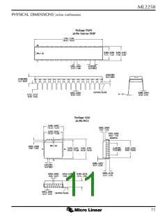
ML2258
The capacitor/resistor array offers fast conversion, superior
linearity and accuracy since matching is only required
1.0 FUNCTIONAL DESCRIPTION
4
8
between 2 = 16 elements (as opposed to 2 = 256
elements in conventional designs). And since the levels are
based on the ratio of capacitors to capacitors and resistors to
resistors, the accuracy and long term stability of the
converter is improved. This also guarantees monotonicity
and no missing codes, as well as eliminating any linearity
temperature or power supply dependence.
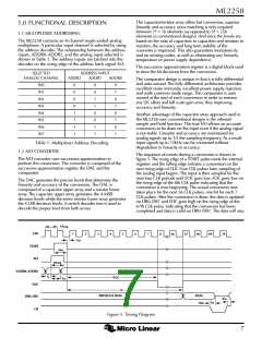
1.1 MULTIPLEXER ADDRESSING
The ML2258 contains an 8-channel single ended analog
multiplexer. A particular input channel is selected by using
the address decoder. The relationship between the address
inputs, ADDR0–ADDR2, and the analog input selected is
shown in Table 1. The address inputs are latched into the
decoder on the rising edge of the address latch signal ALE.
The successive approximation register is a digital block used
to store the bit decisions from the conversion.
SELECTED
ADDRESS INPUT
ANALOG CHANNEL
ADDR2
ADDR1
ADDR0
The comparator design is unique in that it is fully differential
and auto-zeroed. The fully differential architecture provides
excellent noise immunity, excellent power supply rejection,
and wide common mode range. The comparator is auto
zeroed at the start of each conversion in order to remove
any DC offset and full scale gain error, thus improving
accuracy and linearity.
IN0
IN1
IN2
IN3
IN4
IN5
IN6
IN7
0
0
0
0
1
1
1
1
0
0
1
1
0
0
1
1
0
1
0
1
0
1
0
1
Another advantage of the capacitor array approach used in
the ML2258 over conventional designs is the inherent
sample and hold function. This true S/H allows an accurate
conversion to be done on the input even if the analog signal
is not stable. Linearity and accuracy are maintained for
analog signals up to 1/2 the sampling frequency. As a result,
input signals up to 75kHz can be converted without
degradation in linearity or accuracy.
Table 1. Multiplexer Address Decoding
1.2 A/D CONVERTER
The A/D converter uses successive approximation to
perform the conversion. The converter is composed of the
successive approximation register, the DAC and the
comparator.
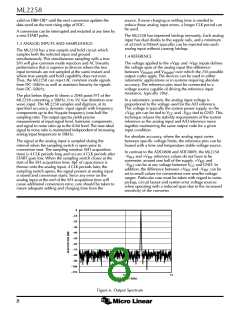
The sequence of events during a conversion is shown in
figure 5. The rising edge of a START pulse resets the internal
registers and the falling edge initiates a conversion on the
next rising edge of CLK. Four CLK pulses later, sampling of
the analog input begins. The input is then sampled for the
next four CLK periods until EOC goes low. EOC goes low on
the rising edge of the 8th CLK pulse indicating that the
conversion is now beginning. The actual conversion now
takes place for the next 56 CLK pulses, one bit for each 7
CLK pulses. After the conversion is done, the data is updated
on DB0–DB7 and EOC goes high on the rising edge of the
67th CLK pulse, indicating that the conversion has been
completed and data is valid on DB0–DB7. The data will stay
The DAC generates the precise levels that determine the
linearity and accuracy of the conversion. The DAC is
composed of a capacitor upper array and a resistor lower
array. The capacitor upper array generates the 4 MSB
decision levels while the series resistor lower array generates
the 4 LSB decision levels. A switch decoder tree is used to
decode the proper level from both arrays.
1/f
CLK
CLK
START
1
2
3
4
5
6
7
8
66
67
68
69
70
t
SS
t
WS
ALE
t
WALE
ADDR0–ADDR2
t
t
S
EOC
t
H
EOC
t
C
PREVIOUS DATA
DATA
DB0–DB7
t
EN
t
t
H
DIS
OE
Figure 5. Timing Diagram
7

 MICRO-LINEAR [ MICRO LINEAR CORPORATION ]