ML2258
1.5 POWER SUPPLY AND REFERENCE DECOUPLING
A 10µF electrolytic capacitor is recommended to bypass
Intermodulation Distortion
With inputs consisting of sine waves at two frequencies,
f and f , any active device with nonlinearities will create
A B
V
to GND, using as short a lead length as possible. In
CC
addition, with clock frequencies above 1MHz, a 0.1µF
distortion products, of order (m+n), at sum and difference
frequencies of mf + nf , where m, n = 0, 1, 2, 3,... .
ceramic disc capacitor should be used to bypass V to
CC
A
B
GND.
Intermodulation terms are those for which m or n is not
equal to zero. The ML2258 (IMD) intermodulation
distortion specification includes the second order terms
If REF+ and REF– inputs are driven by long lines, they
should be bypassed by 0.1µF Ceramic disc capacitors at
the reference pins (pins 12, 16).
(f + f ) and (f – f ) and the third order terms (2f + f ),
A
B
A
B
A
B
(2f – f ), (f + 2f ) and (f – 2f ) only.
A
B
A
B
A
B
1.6 DYNAMIC PERFORMANCE
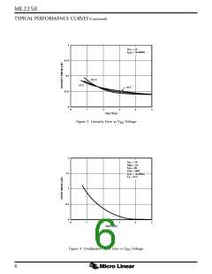
Signal-to-Noise Ratio
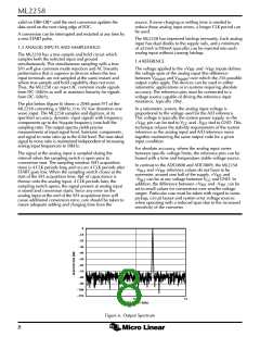
1.7 DIGITAL INTERFACE
The analog inputs are selected by the digital addresses,
ADDR0–ADDR2, and latched on the rising edge of ALE.
This is described in the Multiplexer Addressing section.
Signal-to-noise ratio (SNR) is the measured signal to noise
at the output of the converter. The signal is the rms
magnitude of the fundamental. Noise is the rms sum of all
the nonfundamental signals up to half the sampling
frequency. SNR is dependent on the number of
quantization levels used in the digitization process; the
more levels, the smaller the quantization noise. The
theoretical SNR for a sine wave is given by
A conversion is initiated by the rising edge of a START
pulse. As long as this pulse is high, the internal logic is
reset.
The sampling interval starts with the 4th CLK rising edge
after a START falling edge and ends on the 8th rising edge
of CLK, 4 CLK periods later. On the rising edge of the 8th
CLK pulse, the conversion starts and EOC goes low.
SNR = (6.02N + 1.76)dB
where N is the number of bits. Thus for ideal 8-bit
converter, SNR = 49.92dB.
Each bit conversion in the successive approximation
process takes 7 CLK periods. On the rising edge of the
64th CLK pulse, the digital output of the conversion is
updated on the outputs DB0–DB7. On the rising edge of
the 65th CLK pulse, EOC goes high indicating the
conversion is done and data on DB0–DB7 is valid.
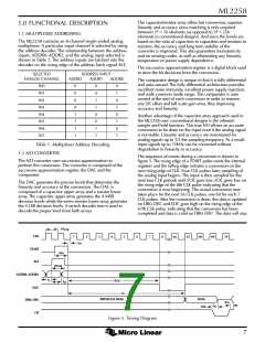
Harmonic Distortion
Harmonic distortion is the ratio of the rms sum of
harmonics to the fundamental. Total harmonic distortion
(THD) of the ML2258 is defined as
One feature of the ML2258 over conventional devices is
that the data is double-buffered. This means that the
outputs DB0–DB7 will stay valid until updated at the end
of the next conversion and will not become invalid when
the next conversion starts. This facilitates interfacing with
external logic of µP.
1/ 2
V22 + V32 + V42 + V52
THD = 20log
V
1
where V is the rms amplitude of the fundamental and V ,
V , V , V are the rms amplitudes of the individual
1
2
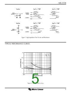
The signal OE drives the data bus, DB0–DB7, into a high
impedance state when held low. This allows the ML2258
to be tied directly to a µP system bus without any latches
or buffers.
3
4
5
harmonics.
9

 MICRO-LINEAR [ MICRO LINEAR CORPORATION ]