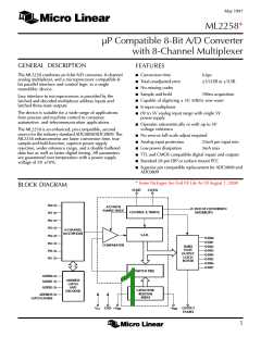
ML2258
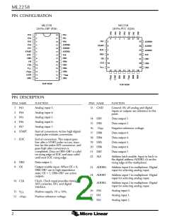
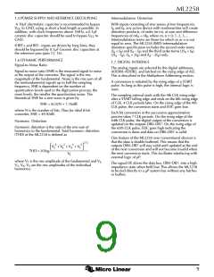
PIN CONFIGURATION
ML2258
ML2258
28-Pin DIP (P28)
28-Pin PCC (Q28)
IN3
IN4
1
2
28
27
26
25
24
23
22
21
20
19
18
17
16
15
IN2
IN1
4
3
2
1
28 27 26
25
IN7
START
EOC
DB3
OE
5
IN5
3
IN0
ADDR0
ADDR1
ADDR2
ALE
IN6
4
ADDR0
ADDR1
ADDR2
ALE
6
24
23
22
21
20
19
IN7
5
7
START
EOC
DB3
OE
6
8
7
8
DB7
9
DB7
9
DB6
CLK
10
11
DB6
CLK
10
11
12
13
14
DB5
V
CC
DB5
V
CC
DB4
12 13 14 15 16 17 18
+V
REF
DB0
GND
DB1
–V
REF
DB2
TOP VIEW
TOP VIEW
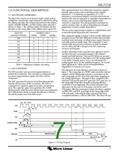
PIN DESCRIPTION
PIN# NAME
FUNCTION
PIN# NAME
13 GND
FUNCTION
1
2
3
4
5
6
IN3
Analog input 3.
Analog input 4.
Analog input 5.
Analog input 6.
Analog input 7.
Ground. 0V, all analog and digital
inputs or outputs are reference to this
point.
IN4
IN5
14 DB1
15 DB2
Data output 1.
IN6
Data output 2.
IN7
16 –V
Negative reference voltage.
Data output 0.
REF
START
Start of conversion. Active high digital
input pulse initiates conversion.
17 DB0
18 DB4
19 DB5
20 DB6
21 DB7
22 ALE
Data output 4.
7
EOC
End of conversion. This output goes
low after a START pulse occurs, stays
low for the entire A/D conversion, and
goes high after conversion is
completed. Data on DB0–DB7 is valid
on rising edge of EOC and stays valid
until next EOC rising edge.
Data output 5.
Data output 6.
Data output 7.
Address latch enable. Input to latch in
the digital address (ADDR2–0) on the
rising edge of the multiplexer.
8
9
DB3
OE
Data output 3.
Output enable input. When OE = 0,
DB0–DB7 are in high impedance
state; OE = 1, DB0–DB7 are active
outputs.
23 ADDR0
24 ADDR1
25 ADDR2
Address input 0 to multiplexer. Digital
input for selecting analog input.
Address input 1 to multiplexer. Digital
input for selecting analog input.
10 CLK
Clock. Clock input provides timing for
A/D converter, S/H, and digital
interface.
Address input 2 to multiplexer. Digital
input for selecting analog input.
26 IN0
27 IN1
28 IN2
Analog input 0.
Analog input 1.
Analog input 2.
11 V
Positive supply. 5V ± 10%.
Positive reference voltage.
CC
12 +V
REF
2

 MICRO-LINEAR [ MICRO LINEAR CORPORATION ]