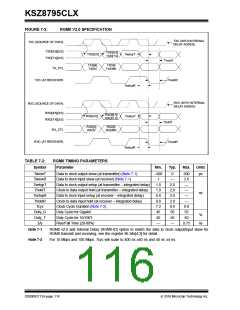
KSZ8795CLX
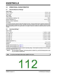
5.0
5.1
OPERATIONAL CHARACTERISTICS
Absolute Maximum Ratings*
Supply Voltage
(VDD12A, VDD12D) ...................................................................................................................................... –0.5V to +1.8V
(VDDAT, VDDIO)........................................................................................................................................... –0.5V to +4.0V
Input Voltage ............................................................................................................................................. –0.5V to +4.0V
Output Voltage........................................................................................................................................... –0.5V to +4.0V
Lead Temperature (soldering, 10s) .......................................................................................................................+260°C
Storage Temperature (TS) ......................................................................................................................–55°C to +150°C
Maximum Junction Temperature...........................................................................................................................+125°C
ESD Rating ................................................................................................................................................................5 kV
*Exceeding the absolute maximum rating may damage the device. Stresses greater than the absolute maximum rating
may cause permanent damage to the device. Operation of the device at these or any other conditions above those spec-
ified in the operating sections of this specification is not implied. Maximum conditions for extended periods may affect
reliability.
5.2
Operating Ratings**
Supply Voltage
(VDD12A, VDD12D) ..............................................................................................................................+1.140V to +1.260V
(VDDAT @ 3.3V).................................................................................................................................+3.135V to +3.465V
(VDDAT @ 2.5V).................................................................................................................................+2.375V to +2.625V
(VDDIO @ 3.3V) .................................................................................................................................+3.135V to +3.465V
(VDDIO @ 2.5V) .................................................................................................................................+2.375V to +2.625V
(VDDIO @ 1.8V) .................................................................................................................................+1.710V to +1.890V
Ambient Temperature (TA)
Commercial ..................................................................................................................................................0°C to +70°C
Industrial...................................................................................................................................................–40°C to +85°C
Package Thermal Resistance (ΘJA, Note 5-1).............................................................................................. +55.05°C/W
Package Thermal Resistance (ΘJC, Note 5-1).............................................................................................. +25.06°C/W
**The device is not guaranteed to function outside its operating ratings. Unused inputs must always be tied to an appro-
priate logic voltage level (GND or VDD).
Note 5-1
Note:
No heat spreader in package. The thermal junction-to-ambient (ΘJA) and the thermal junction-to-case
(ΘJC) are under air velocity 0m/s.
Do not drive input signals without power supplied to the device.
DS00002112A-page 112
2016 Microchip Technology Inc.

 MICREL [ MICREL SEMICONDUCTOR ]