KSZ8795CLX
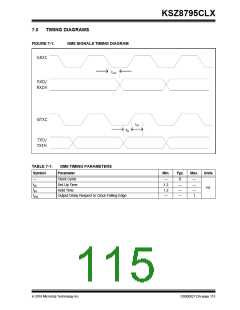
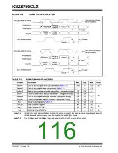
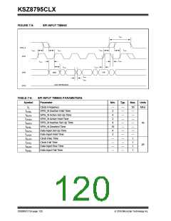
FIGURE 7-2:
RGMII V2.0 SPECIFICATION
TXC (WITH INTERNAL
DELAY ADDED)
TXC (SOURCE OF DATA)
TXD[8:5][3:0]
TXD[7:4][3:0]
TXD[8:5]
TXD[7:4]
TXD[3:0]
TsetupT
TholdT
TXD[4]
TXEN
TXD[9
TXERR
TX_CTL
TXC (AT RECEIVER)
TholdR
TsetupR
TsetupT
RXC (WITH INTERNAL
DELAY ADDED)
RXC (SOURCE OF DATA)
RXD[8:5][3:0]
RXD[7:4][3:0]
RXD[8:5]
RXD[7:4]
RXD[3:0]
TholdT
RXD[4]
RXDV
RXD[9
RXERR
RX_CTL
RXC (AT RECEIVER)
TholdR
TsetupR
TABLE 7-2:
Symbol
RGMII TIMING PARAMETERS
Parameter
Min.
Typ.
Max.
Units
TskewT
TskewR
TsetupT
TholdT
TsetupR
TholdR
Tcyc
Data to clock output skew (at transmitter) (Note 7-1)
Data to clock input skew (at receiver) (Note 7-1)
Data to clock output setup (at transmitter – integrated delay)
Clock to data output hold (at transmitter – integrated delay)
Data to clock input setup (at receiver – integrated delay)
Clock to data input hold (at receiver – integrated delay)
Clock Cycle Duration (Note 7-2)
–500
1
0
500
2.6
—
ps
—
1.0
1.0
0.8
0.8
7.2
45
2.0
2.0
2.0
2.0
8.0
50
50
—
—
ns
—
—
8.8
55
Duty_G
Duty_T
tr/tf
Duty Cycle for Gigabit
%
Duty Cycle for 10/100T
40
60
Rise/Fall Time (20-80%)
—
0.75
ns
Note 7-1
RGMII v2.0 add Internal Delay (RGMII-ID) option to match the data to clock output/input skew for
RGMII transmit and receiving, see the register 86 bits[4:3] for detail.
Note 7-2
For 10 Mbps and 100 Mbps. Tcyc will scale to 400 ns ±40 ns and 40 ns ±4 ns.
DS00002112A-page 116
2016 Microchip Technology Inc.

 MICREL [ MICREL SEMICONDUCTOR ]