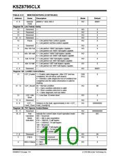
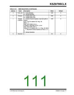
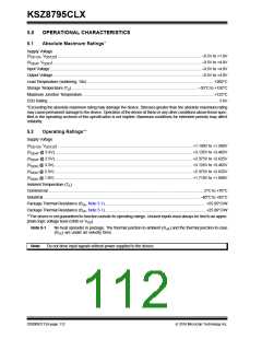
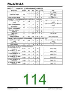
KSZ8795CLX
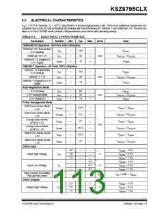
TABLE 6-1:
ELECTRICAL CHARACTERISTICS (CONTINUED)
Parameters
Symbol
Min.
Typ.
Max.
Units
Note
—
—
—
—
—
—
—
—
0.4
0.4
0.3
10
VDDIO = 3.3V
Output Low Voltage
VOL
IOZ
V
V
DDIO = 2.5V
DDIO = 1.8V
V
Output Tri-State Leakage
µA
VIN = GND ~ VDDIO
100BASE-TX Transmit (measured differentially after 1:1 transformer)
Peak Differential Output
100ꢀ termination on the differential
VO
0.95
—
—
—
1.05
2
V
Voltage
output
100ꢀ termination on the differential
Output Voltage Imbalance
VIMB
%
output
Rise/Fall Time
Rise/Fall Time Imbalance
Duty Cycle Distortion
Overshoot
3
0
—
—
5
0.5
±0.5
5
—
tr/tf
ns
—
—
—
—
—
—
0
—
ns
%
—
—
—
Output Jitters
0.75
1.4
ns
Peak-to-Peak
10BASE-T Receive
Squelch Threshold
VSQ
300
400
585
mV
5 MHz square wave
10BASE-T Transmit (measured differentially after 1:1 transformer) VDDAT = 3.3V
Peak Differential Output
Voltage
100ꢀ termination on the differential
VP
2.2
2.5
2.8
V
output
Peak-to-Peak
—
Output Jitters
—
—
—
—
1.4
28
3.5
30
ns
ns
Rise/Fall Times
I/O Pin Internal Pull-Up and Pull-Down Resistance
I/O Pin Effective Pull-Up
R1.8PU
R1.8PD
R2.5PU
R2.5PD
R3.3PU
R3.3PD
75
53
46
46
35
37
95
68
60
59
45
46
135
120
93
VDDIO = 1.8V
VDDIO = 1.8V
VDDIO = 2.5V
VDDIO = 2.5V
VDDIO = 3.3V
VDDIO = 3.3V
Resistance
I/O Pin Effective Pull-Down
Resistance
I/O Pin Effective Pull-Up
Resistance
kꢀ
I/O Pin Effective Pull-Down
Resistance
103
65
I/O Pin Effective Pull-Up
Resistance
I/O Pin Effective Pull-Down
Resistance
74
DS00002112A-page 114
2016 Microchip Technology Inc.

 MICREL [ MICREL SEMICONDUCTOR ]