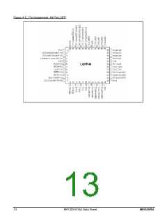
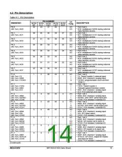
(Continued)
PIN NUMBER
I/O
TYPE
MNEMONIC
DESCRIPTION
40-Pin 44-Pin 44-Pin 48-Pin 28-Pin
DIP
PLCC
PQFP
LQFP
SSOP
P4.0
P4.1
(Alt. Fun.) ALE
-
-
23
34
17
28
18
31
-
I/O
I/O
O
* Port 4 bit-0.
* Port 4 bit-1.
* ALE: Address Latch Enable, output
pulse for latching the low byte of the
address during an access to external
data memory.
P4.2
(Alt. Fun.) /INT3
P4.3
(Alt. Fun.) /INT2
P4.4
P4.5
P4.6
P4.7
-
-
1
39
6
42
7
1
-
I/O
I
I/O
I
I/O
I/O
I/O
I/O
* Port 4 bit-2.
* /INT3: external interrupt 3 input.
* Port 4 bit-3.
* /INT2: external interrupt 2 input.
* Port 4 bit-4.
* Port 4 bit-5.
* Port 4 bit-6.
* Port 4 bit-7.
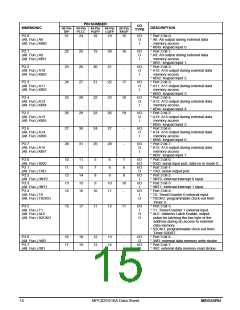
12
-
-
-
-
-
-
-
-
-
24
25
48
1
-
-
-
-
-
-
-
OCD_SDA
OCD_SCL
XTAL1
30
29
19
33
32
21
27
26
15
30
29
16
21
20
13
I/O
I
I
On-Chip Debug Interface, serial data.
On-Chip Debug Interface, serial clock.
Crystal1: input to the inverting oscillator
amplifier and input to the internal clock
generator circuits.
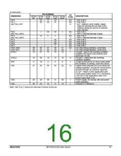
XTAL2
RST
18
9
20
10
35
14
4
15
5
12
6
O
I
Crystal 2: output from the inverting
oscillator amplifier.
A high on this pin for 24 clock cycles while
the oscillator is running, resets the device.
Output of the internal LDO (Low Drop-Out
voltage regulator): should be connected to
ground through an external capacitor
(4.7μF~100μF) in the application with
VDD power higher than 3.6V; and tied to
VDD pin in the application with VDD
power lower than 3.6V.
V30
31
29
32
22
O
VDD
VSS
40
20
44
22
38
16
41
17
28
14
I
I
Power supply, for normal, idle and power-
down operation.
Ground, 0 V reference.
Note: “(Alt. Fun.)” means the Alternate Function of this pin.
MEGAWIN
MPC82G516A Data Sheet
16

 MEGAWIN [ MEGAWIN TECHNOLOGY CO., LTD ]