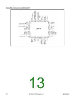
PIN NUMBER
40-Pin 44-Pin 44-Pin 48-Pin 28-Pin
I/O
TYPE
MNEMONIC
DESCRIPTION
DIP
PLCC
PQFP
LQFP
SSOP
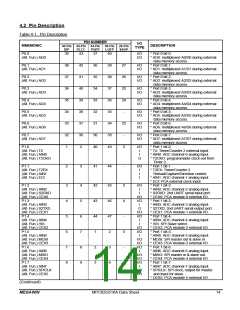
P2.0
(Alt. Fun.) A8
(Alt. Fun.) KBI0
21
24
18
19
15
I/O
O
I
* Port 2 bit-0.
* A8: A8 output during external data
memory access.
* KBI0: keypad input 0.
P2.1
(Alt. Fun.) A9
(Alt. Fun.) KBI1
22
23
24
25
26
27
28
25
26
27
28
29
30
31
19
20
21
22
23
24
25
20
21
22
23
26
27
28
16
-
I/O
O
I
* Port 2 bit-1.
* A9: A9 output during external data
memory access.
* KBI1: keypad input 1.
* Port 2 bit-2.
* A10: A10 output during external data
memory access.
* KBI2: keypad input 2.
* Port 2 bit-3.
* A11: A11 output during external data
memory access.
* KBI3: keypad input 3.
* Port 2 bit-4.
* A12: A12 output during external data
memory access.
* KBI4: keypad input 4.
* Port 2 bit-5.
* A13: A13 output during external data
memory access.
* KBI5: keypad input 5.
* Port 2 bit-6.
P2.2
(Alt. Fun.) A10
(Alt. Fun.) KBI2
I/O
O
I
P2.3
(Alt. Fun.) A11
(Alt. Fun.) KBI3
17
18
19
-
I/O
O
I
P2.4
(Alt. Fun.) A12
(Alt. Fun.) KBI4
I/O
O
I
P2.5
(Alt. Fun.) A13
(Alt. Fun.) KBI5
I/O
O
I
P2.6
(Alt. Fun.) A14
(Alt. Fun.) KBI6
I/O
O
I
* A14: A14 output during external data
memory access.
* KBI6: keypad input 6.
* Port 2 bit-7.
* A15: A15 output during external data
memory access.
P2.7
(Alt. Fun.) A15
(Alt. Fun.) KBI7
-
I/O
O
I
* KBI7: keypad input 7.
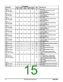
P3.0
(Alt. Fun.) RXD
P3.1
(Alt. Fun.) TXD
P3.2
(Alt. Fun.) /INT0
P3.3
(Alt. Fun.) /INT1
P3.4
(Alt. Fun.) T0
(Alt. Fun.) T0CKO
10
11
12
13
14
11
13
14
15
16
5
7
6
8
7
8
I/O
I/O
I/O
O
I/O
I
I/O
I
I/O
I
* Port 3 bit-0.
* RXD: serial input port, data i/o in mode 0.
* Port 3 bit-1.
* TXD: serial output port.
* Port 3 bit-2.
* /INT0: external interrupt 0 input.
* Port 3 bit-3.
* /INT1: external interrupt 1 input.
* Port 3 bit-4.
* T0: Timer/Counter 0 external input.
* T0CKO: programmable clock-out from
Timer 0.
8
9
9
9
10
11
10
-
10
O
P3.5
15
17
11
12
11
I/O
I
O
O
* Port 3 bit-5.
(Alt. Fun.) T1
(Alt. Fun.) ALE
(Alt. Fun.) S2CKO
* T1: Timer/Counter 1 external input.
* ALE: Address Latch Enable, output
pulse for latching the low byte of the
address during an access to external
data memory.
* S2CKO: programmable clock-out from
Timer S2BRT.
P3.6
(Alt. Fun.) /WR
P3.7
(Alt. Fun.) /RD
16
17
18
19
12
13
13
14
-
-
I/O
O
I/O
O
* Port 3 bit-6.
* /WR: external data memory write strobe.
* Port 3 bit-7.
* /RD: external data memory read strobe.
15
MPC82G516A Data Sheet
MEGAWIN

 MEGAWIN [ MEGAWIN TECHNOLOGY CO., LTD ]