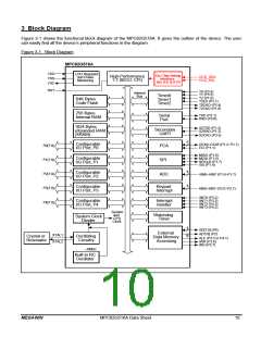
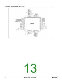
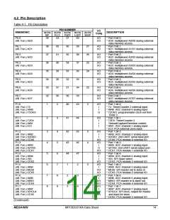
4.2 Pin Description
Table 4-1. Pin Description
PIN NUMBER
40-Pin 44-Pin 44-Pin 48-Pin 28-Pin
I/O
TYPE
MNEMONIC
DESCRIPTION
DIP
PLCC
PQFP
LQFP
SSOP
P0.0
(Alt. Fun.) AD0
39
43
37
40
-
I/O
I/O
* Port 0 bit-0.
* AD0: multiplexed A0/D0 during external
data memory access.
P0.1
(Alt. Fun.) AD1
38
37
36
35
34
33
32
1
42
41
40
39
38
37
36
2
36
35
34
33
32
31
30
40
39
38
37
36
35
34
33
43
27
26
25
24
-
I/O
I/O
* Port 0 bit-1.
* AD1: multiplexed A1/D1 during external
data memory access.
* Port 0 bit-2.
* AD2: multiplexed A2/D2 during external
data memory access.
* Port 0 bit-3.
* AD3: multiplexed A3/D3 during external
data memory access.
* Port 0 bit-4.
* AD4: multiplexed A4/D4 during external
data memory access.
* Port 0 bit-5.
* AD5: multiplexed A5/D5 during external
data memory access.
* Port 0 bit-6.
* AD6: multiplexed A6/D6 during external
data memory access.
* Port 0 bit-7.
* AD7: multiplexed A7/D7 during external
data memory access.
P0.2
(Alt. Fun.) AD2
I/O
I/O
P0.3
(Alt. Fun.) AD3
I/O
I/O
P0.4
(Alt. Fun.) AD4
I/O
I/O
P0.5
(Alt. Fun.) AD5
I/O
I/O
P0.6
(Alt. Fun.) AD6
23
-
I/O
I/O
P0.7
(Alt. Fun.) AD7
I/O
I/O
P1.0
2
I/O
* Port 1 bit-0.
(Alt. Fun.) T2
(Alt. Fun.) AIN0
(Alt. Fun.) T2CKO
I
I
O
* T2: Timer/Counter 2 external input.
* AIN0: ADC channel-0 analog input.
* T2CKO: programmable clock-out from
Timer 2.
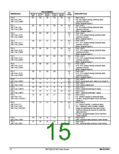
P1.1
2
3
41
44
-
I/O
* Port 1 bit-1.
(Alt. Fun.) T2EX
(Alt. Fun.) AIN1
(Alt. Fun.) ECI
I
I
I
* T2EX: Timer/Counter 2
Reload/Capture/Direction control.
* AIN1: ADC channel-1 analog input.
* ECI: PCA external clock input.
* Port 1 bit-2.
* AIN2: ADC channel-2 analog input.
* S2RXD: 2nd UART serial input port.
* CEX0: PCA module-0 external I/O.
* Port 1 bit-3.
* AIN3: ADC channel-3 analog input.
* S2TXD: 2nd UART serial output port.
* CEX1: PCA module-1 external I/O.
* Port 1 bit-4.
* AIN4: ADC channel-4 analog input.
* /SS: SPI Slave select.
P1.2
3
4
5
6
7
8
4
5
6
7
8
9
42
43
44
1
45
46
47
2
3
4
-
I/O
I
I
I/O
I/O
I
(Alt. Fun.) AIN2
(Alt. Fun.) S2RXD
(Alt. Fun.) CEX0
P1.3
(Alt. Fun.) AIN3
(Alt. Fun.) S2TXD
(Alt. Fun.) CEX1
P1.4
(Alt. Fun.) AIN4
(Alt. Fun.) /SS
(Alt. Fun.) CEX2
P1.5
(Alt. Fun.) AIN5
(Alt. Fun.) MOSI
(Alt. Fun.) CEX3
P1.6
(Alt. Fun.) AIN6
(Alt. Fun.) MISO
(Alt. Fun.) CEX4
P1.7
(Alt. Fun.) AIN7
(Alt. Fun.) SPICLK
(Alt. Fun.) CEX5
O
I/O
I/O
I
I
I/O
I/O
I
I/O
I/O
I/O
I
I/O
I/O
I/O
I
I/O
I/O
* CEX2: PCA module-2 external I/O.
* Port 1 bit-5.
5
-
* AIN5: ADC channel-5 analog input.
* MOSI: SPI master out & slave in.
* CEX3: PCA module-3 external I/O.
* Port 1 bit-6.
* AIN6: ADC channel-6 analog input.
* MISO: SPI master in & slave out.
* CEX4: PCA module-4 external I/O.
* Port 1 bit-7.
2
3
3
4
-
* AIN7: ADC channel-7 analog input.
* SPICLK: SPI clock, output for master
and input for slave.
* CEX5: PCA module-5 external I/O.
(Continued)
MEGAWIN
MPC82G516A Data Sheet
14

 MEGAWIN [ MEGAWIN TECHNOLOGY CO., LTD ]