MX26C1000B
effects of the printed circuit board traces on EPROM
arrays, a 4.7 uF bulk electrolytic capacitor should be
used between VCC and GND for each of the eight
devices. The location of the capacitor should be close
to where the power supply is connected to the array.
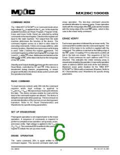
OUTPUT DISABLE
Output is disabled when OE is at logre high. When in
outputdisabledallcircuitryisenabled.Excepttheoutput
pins are in a high impedance state(TRI-ATATE).
Table 1: BUS OPERATIONS
Mode
VPP(1)
A0
A0
X
A9
A9
X
CE
VIL
VIL
VIH
OE
VIL
VIH
X
WE
VIH
VIH
X
Q0~Q7
Read
VPPL
VPPL
VPPL
VPPL
VPPL
VPPH
VPPH
VPPH
VPPH
Data Out
Tri-State
Tri-State
Data=C2H
Data=CFH
DataOut(3)
Tri-State
Tri-State
Data Inb
READ-ONLY
MODE
OutputDisable
Standby
X
X
ManufacturerIdentification
Device Identification
Read
VIL
VID(2) VIL
VIL
VIL
VIL
VIH
X
VIH
VIH
VIH
VIH
X
VIH VID(2) VIL
A0
X
A9
X
VIL
VIL
VIH
VIL
COMMAND
MODE
OutputDisable
Standby(4)
X
X(5)
A9
Program
A0
VIH
VIL
Note:
1. Refer to DC Characteristics. When VPP=VPPL memory contents can be read but not written or erased.
2. VID is the intelligent identifier high voltage. Refer to DC Characteristics.
3. Read operations with VPP=VPPH may access array data or the intelligent identifier codes.
4. With VPP at high voltage the standby current equals ICC+IPP(standby).
5. Refer to Table 2 for vaild data-in during a write operation.
6. X can be VIL or VIH.
REV. 0.6, OCT. 04, 2001
P/N: PM0767
5

 Macronix [ MACRONIX INTERNATIONAL ]