MX26C1000B
Theset-upProgramcommand(40H)istheonlycommand
thatrequiresatwosequenceresetcycle.ThefirstReset
commandisinterpretedasprogramdata.However,FFH
dataisconsiderednulldataduringprogrammingoperations
(memory cells are only programmed from logica "1" to
"0". The second Reset command safely aborts the
programming operation and resets the device to the
Readmode.
FUNCTIONAL DESCRIPTION
When the MX26C1000B is delivered, or it is erased, the
chip has all 1000K bits in the "ONE", or HIGH state.
"ZEROs" are loaded into the MX26C1000B through the
procedure of programming.
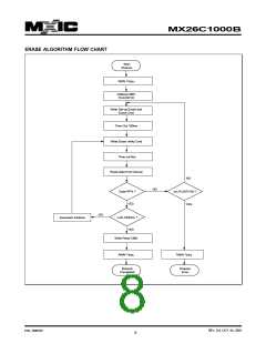
ERASE ALGORITHM
This detailed information is for your reference. It may
prove esier to always issue the Reset command two
consecutivetimes.Thiseliminatestheneedtodetermine
if you are in the set-up Program state or not.
The MX26C1000B do not required preprogramming
beforeaneraseoperation.Theerasealgorithmisaclose
loop flow to simultaneously erase all bits in the entire
array. Erase operation starts with the initial erase
operation. Erase verification begins at address 0000H
by reading data FFH from each byte. If any byte fails
to erase. the entire chip is reerased. to a maximum for
30 pulse counts of 100ms duration for each pulse. The
maximum cumulative erase time is 3s. However. the
deviceisusuallyerasedinnomorethan3pulses. Erase
verification time can be reduced by storing the address
of the last byte that failed. Following the next erase
operation verification may start at the stored address
location. JEDEC standard erase algorithm can also be
used. But erase time will increase by performing the
unnecessarypreprogramming.
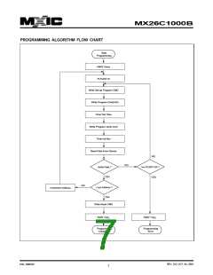
SET-UP PROGRAM/PROGRAM
A three-step sequence of commands is required to
performacompleteprogramoperation:SetUpProgram-
Program-ProgramVerify.Thedeviceisbulkerasedand
bytebybyteprogramming.Thecommand40Hiswritten
to the command register to initiate Set Up Program
operation. Address and data to be programmed into the
byte are provided on the second WE pulse. Addresses
arelatchedonthefallingedgeoftheWEpulse, dataare
latched on the rising edge of the WE pulse. Program
operation begins on the rising edge of the second WE
pulse, and terminate of the next rising edge of the WE
pulse. Refer to AC Characteristics and Waveforms for
specific timing parameters.
PROGRAM ALGORITHM
The device is programmed byte by byte. A maximum
of 25 pulses. each of 10us duration is allowed for each
byte being programmed. The byte may be programmed
sequentially or by random. After each program pulse,
a program verify is done to determine if the byte has
been successfully programmed.
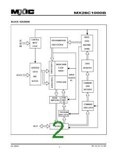
COMMAND REGISTER
When high voltage is applied to VPP the command
registerisenabled.Read,write,standby,outputdisable
modes are available. The read, erase, erase verify,
program,programverifyandDeviceIDareaccessedvia
the command register. Standard microprocessor write
timingsareusedtoinputacommandtotheregister.This
register serves as the input to an internal state machine
which controls the operation mode of the device. An
internal latch is used for write cycles, addresses and
dataforprogramminganderaseoperations.
Programming then proceeds to the next desired byte
location. JEDEC standard program algorithms can be
used.
RESET
The Reset command initializes the MTP EPROMTM
devicetotheReadmode.Inaddition,italsoprovidesthe
user with a safe method to abort any device operation
(includingprogramorerase).TheResetcommandmust
bewrittentwoconsecutivetimesaftertheset-upProgram
command (40H). This will safely abort any previous
operation and initialize the device to the Read mode.
NO INTEGRATED STOP TIMER FOR ERASE
Leading industry flash technology requires a stop timer
built into the flash chip to prevent the memory cells from
going into depletion due to over erase. The 1 Mbit MTP
REV. 0.6, OCT. 04, 2001
P/N: PM0767
3

 Macronix [ MACRONIX INTERNATIONAL ]